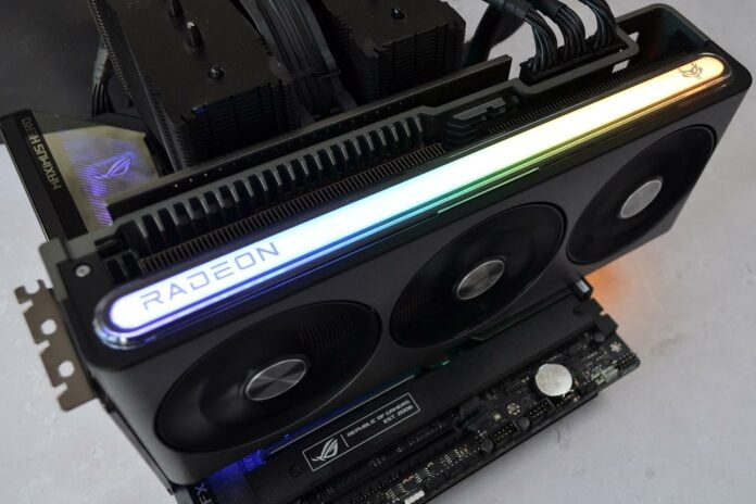
Hot on the heels of the Radeon RX 7900 XTX big reveal last week, add-in board partners have been busy releasing their own takes on AMD’s finest consumer graphics card. The Made By AMD (MBA) card is impressive enough in its own right, but the stealthy black aesthetic lacks the wow factor associated with prime aftermarket designs.

Sapphire Nitro+ RX 7900 XTX Vapor-X
£1,199
Pros
- Fantastic lighting
- So cool and quiet
- Great overall design
- Overclocks well
- Smashes RX 6950 XT
Cons
- Ray tracing remains weak
Club386 may earn an affiliate commission when you purchase products through links on our site.
How we test and review products.
Looking to set the record straight, Sapphire has released it’s own take on AMD’s best graphics card with the Radeon RX 7900 XTX Nitro+ Vapor-X. Bettering ever-improving reference board designs is fast becoming difficult for add-in partners, nevertheless, with a rich history of innovation and design within Pulse, Nitro+, and Toxic families, the Hong Kong-based company has always remained a step ahead.
Radeon RX 7900 XTX is initially offered in Pulse and Nitro+ guises. Both exceed AMD’s 2,500MHz XTX boost speed by clocking in at 2,525MHz and 2,680MHz, respectively. It’s to the £1,200 Nitro+ Vapor-X we draw attention.
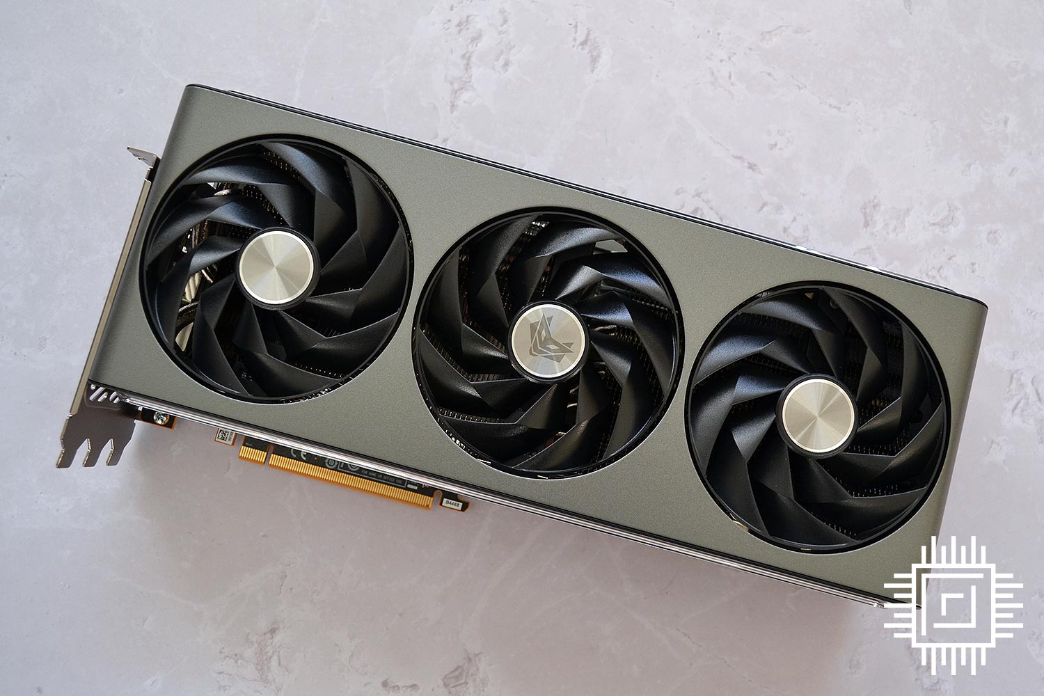
There’s little incentive for Sapphire to ape the MBA board’s design. Going bigger and taller with measurements of 320mm length, 135.75mm width and 71.6mm height – equating to a 3.5-slot card in normal parlance – Sapphire uses the same Nitro+ design on XTX and XT variants.
The hefty monster’s higher frequencies result in elevated power levels of up to 420W for the entire card, compared to 355W attributed to MBA. We say up to because being a Nitro+ card means there’s a three-position switch which toggles frequencies.
Sapphire’s default position enables switching of primary and secondary modes through TriXX software. The next position is the one to head for when guaranteeing headline frequencies of 2,680MHz boost. Shifting over to the third setting, meanwhile, reduces boost speed to 2,500MHz – matching AMD’s card – and removes approximately 50W of board power, though quite why you’d want to run Nitro+ Vapor-X slowly begs a different question.
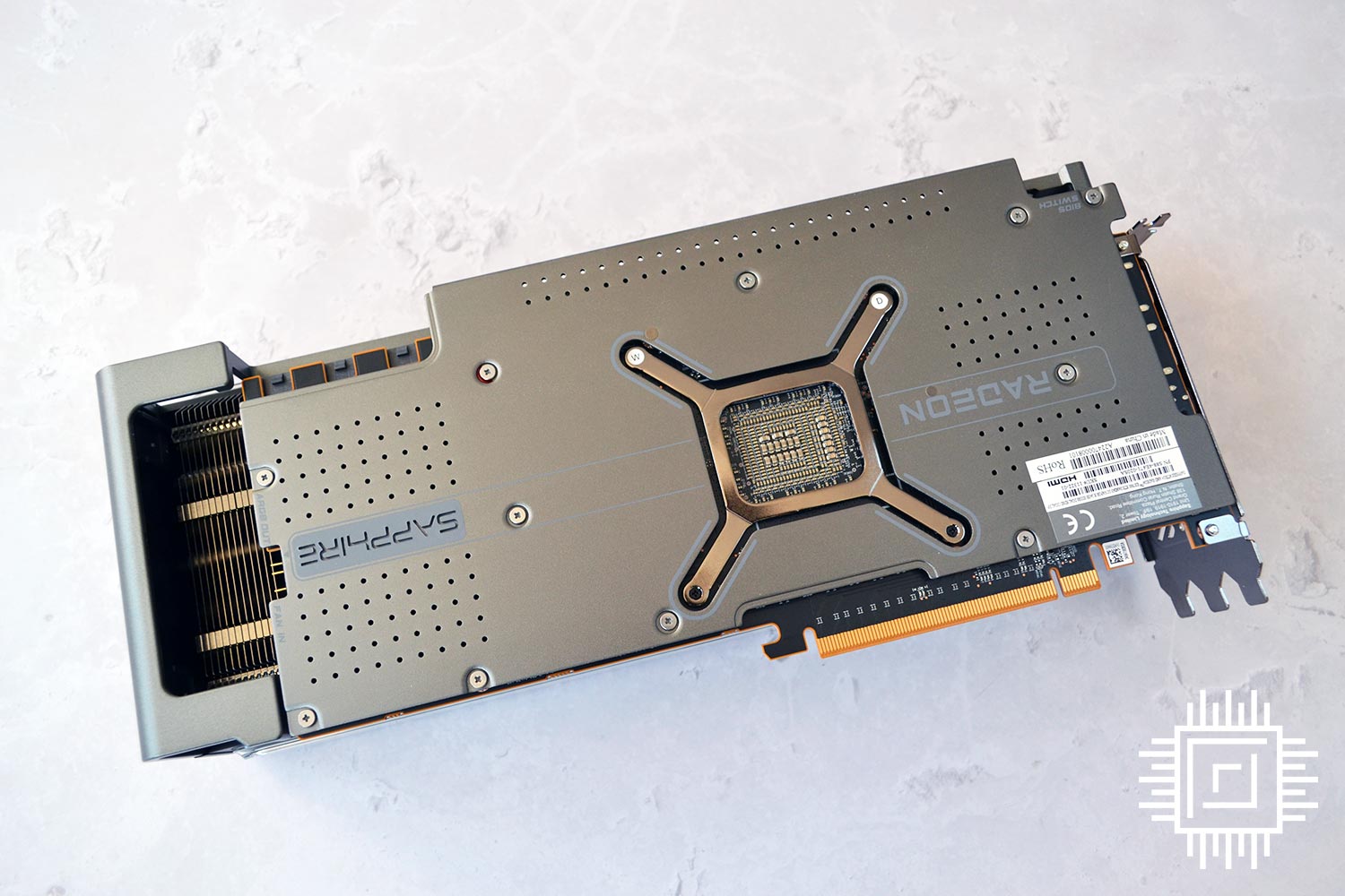
Sapphire uses an MBA-matching 20-phase power supply for the card, with 17 heading to the GPU and three for memory. Rated at up to 70A each, good luck in getting close to 1,400W! Overkill in a good way.
Let’s not beat around the bush. Sapphire’s all-new heatsink design is a delight. The die-cast aluminium frame carries three axial fans using a dual ball-bearing design. Part of the Quick Connect range, the fans can be removed individually for maintenance and cleaning purposes. The trio switch off at temperatures below 50°C and then ramp up in very orderly fashion, helped by what Sapphire says are the tightest fan-speed tolerances to date.
We observed none of the sawtooth fan-speed issues afflicting lesser solutions also carrying a zero-RPM mode; the switch between idle and higher speeds is graceful and barely detectable, even in a quiet system such as our test rig.
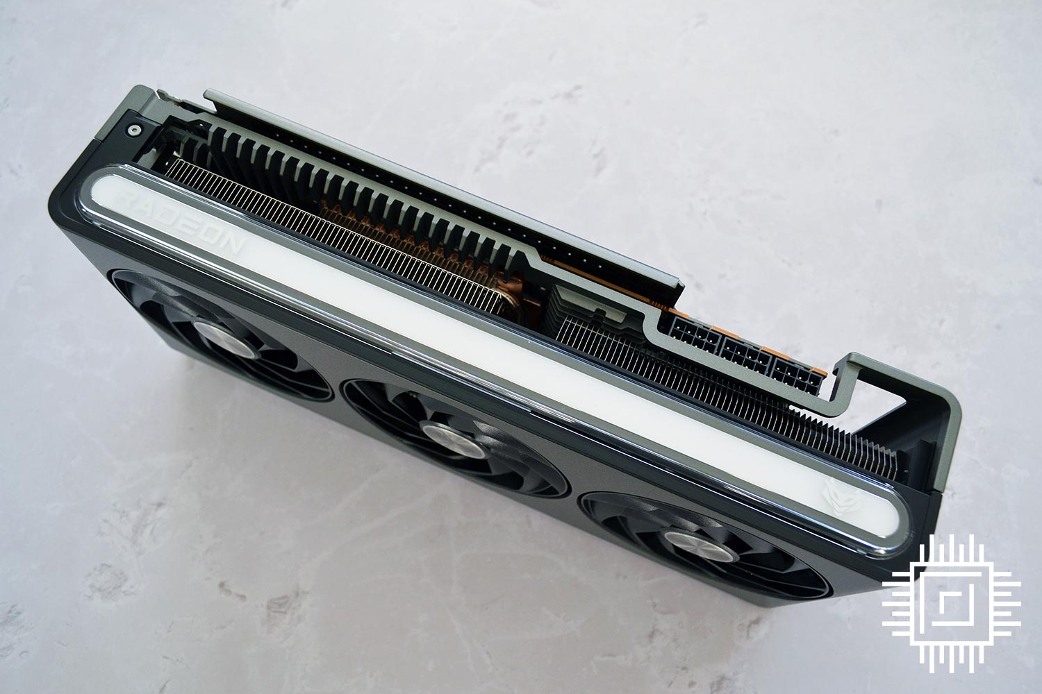
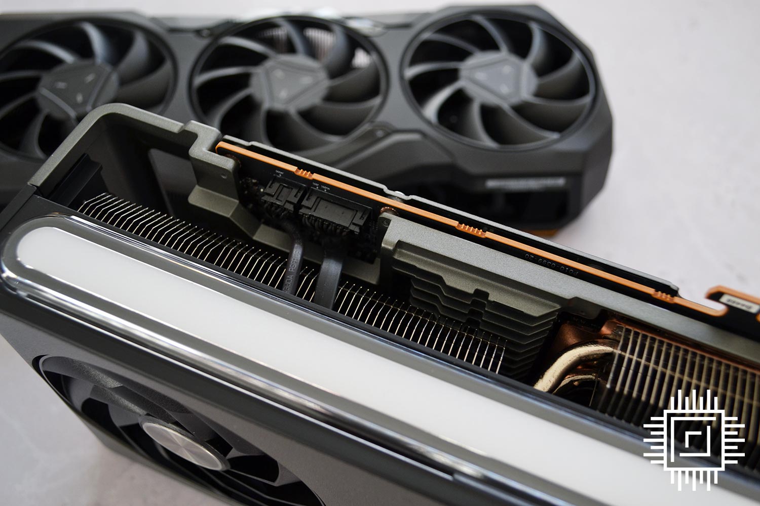
AMD makes quite the noise about having only two 8-pin connectors on the MBA card; Sapphire sees things differently by using three plugs enabling 525W with ease. Certainly makes sense for an overclocked card, though one can argue the single-cable 12VHPWR connector, favoured by Nvidia and capable of 600W, facilitates a tidier build.
Nitro+ Vapor-X is an imposing solution weighing a substantial 1,955g. Rather than imbue fans with obligatory RGB lighting, Sapphire takes a different tack to previous designs, as presentation is quite different to, say, the RX 6950 XT Nitro+ Pure.
Instead, the 71.6mm height comes in useful as we’re treated to impressive ARGB light bars on both sides of the heatsink. Controlled by Trixx software, the colourway can be set to various telemetry, including fan speed or PCB temperature. Those wanting to synchronise with the rest of the system can do so with a three-pin ARGB header and cable to the motherboard.
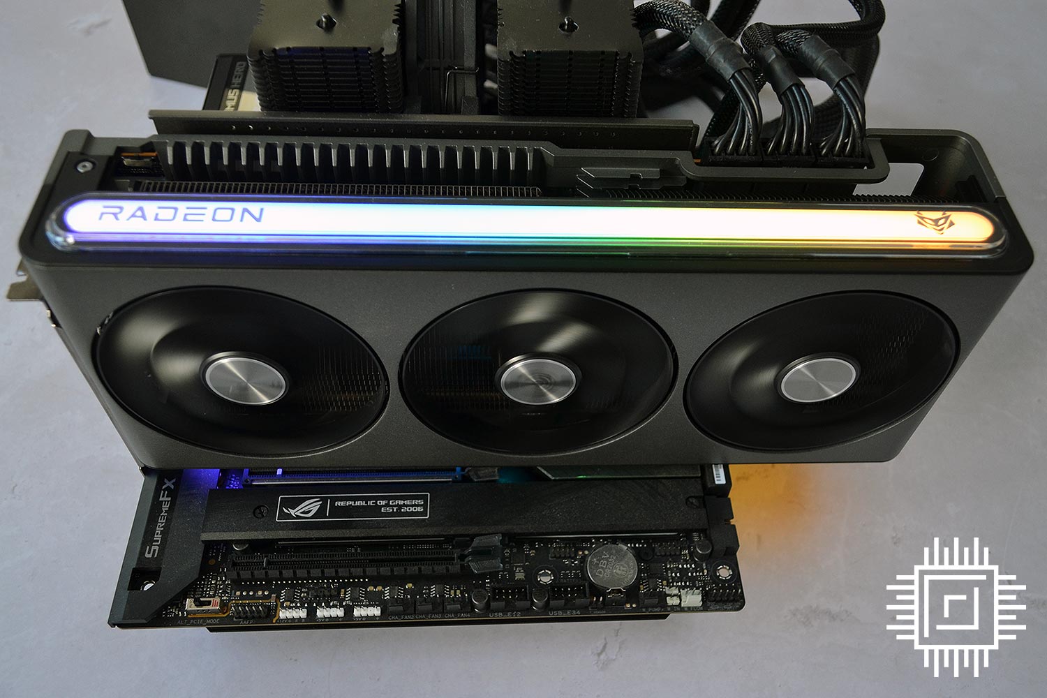
Having a minimalistic shroud and lightbar-accentuated lighting works fantastically well, lending the card a high-quality look, with further RGB behind the Sapphire logo on the rear. Sweeping gradually from one side to the other, out-the-box effects are smooth and without hotspots typically seen on poorer designs. It’s hypnotic to see waves of RGB run across the device.
As the lightbar is present on both sides in equal measure, mounting a card in normal orientation results in identical illumination, though bouncing off the motherboard and chassis, the effect is perceived differently. Top marks to Sapphire’s implementation.
Our benchmark results are in, but it would be remiss not to first revisit what’s under the hood. Here’s a recap on everything you need to know about how AMD has gone about building a chiplet-based GPU architecture endowed with RDNA 3 goodness.
RDNA 3 – Faster And Smarter
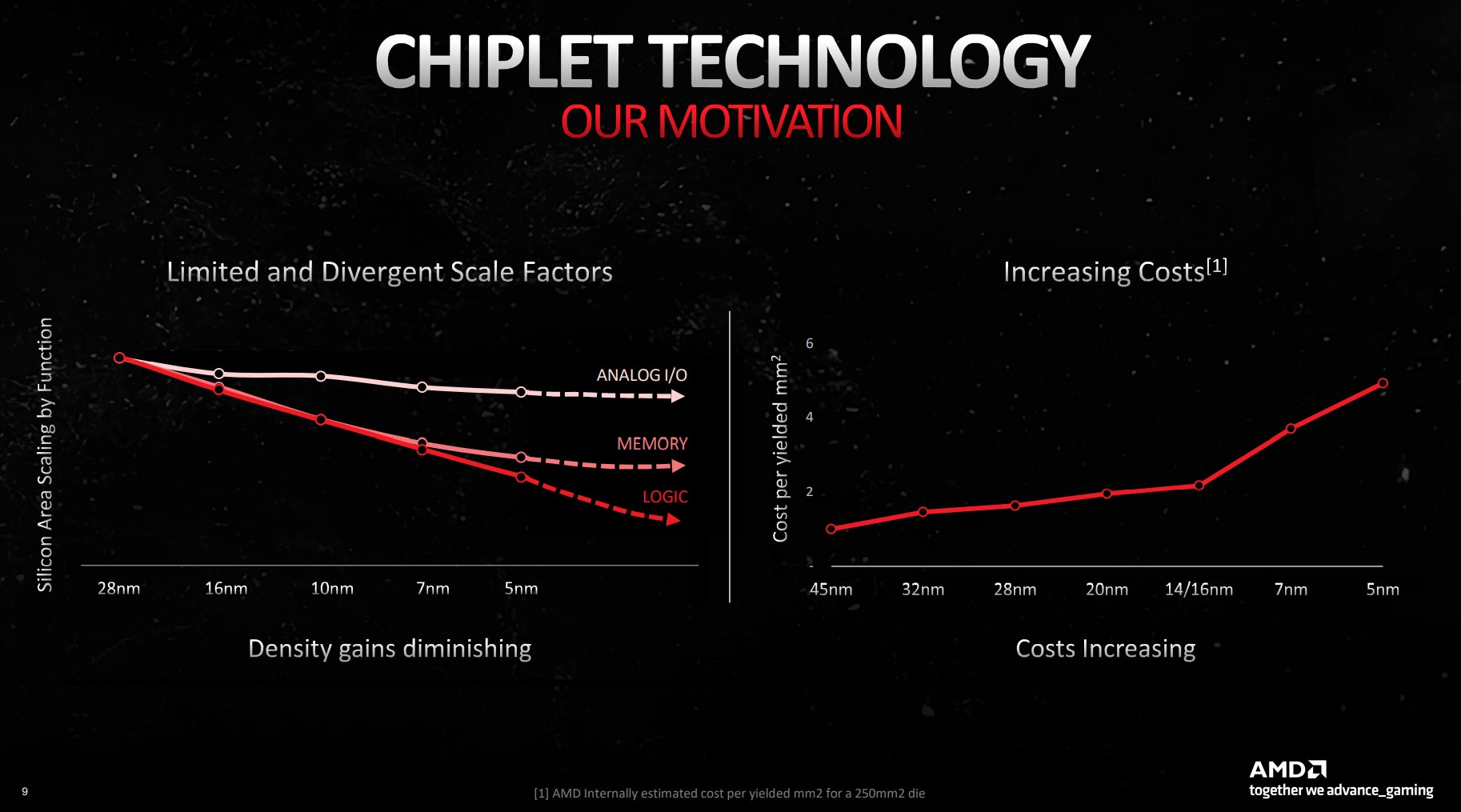
Understanding the impetus behind AMD’s newest GPU architecture first requires an appreciation of two factors affecting the production of cutting-edge silicon. As we move down to ever-smaller nodes, the first is a lack of scaling in two important metrics: memory and analogue I/O, both of which are liberally used in GPU design.
a strategy that has worked wonders in the CPU space with chiplet-based Ryzen processors since 2017
The point here is it’s not worth having these two facets on the latest, most expensive nodes if there is no immediate benefit to doing so, because you’re paying over the odds for no discernible benefit. On the other hand, logic – the building blocks for the core blocks – appears to still scale well, meaning it’s worth investing in smaller processors for attendant gains.
The second point is related to the first insofar as the cost of moving between the latest nodes is becoming significantly more expensive. Only use, say, 5nm production if you absolutely have to, as while it makes powerful chips physically feasible, there comes a time when they’re not financially viable. For example, building a monster, monolithic 700mm² die on purely 5nm is an exercise in inflating end-user cost to arguably unpalatable levels.
Such thinking coalesces into AMD’s fundamental fabrication strategy for high-end graphics moving forwards. Knowing GPUs are essentially huge calculators processing instructions in parallel, why not break down the constituent parts of the design into small blocks, which naturally yield better, and lasso them together with high-speed smarts? It’s a strategy that has worked wonders in the CPU space with chiplet-based Ryzen processors since 2017. But if something was easy, it would have been implemented by now.
GPU Chiplets Provide Unique Challenges
Though brilliant on paper, there are myriad reasons why a chiplet-based GPU is a difficult proposition, exemplified by the graphic below.
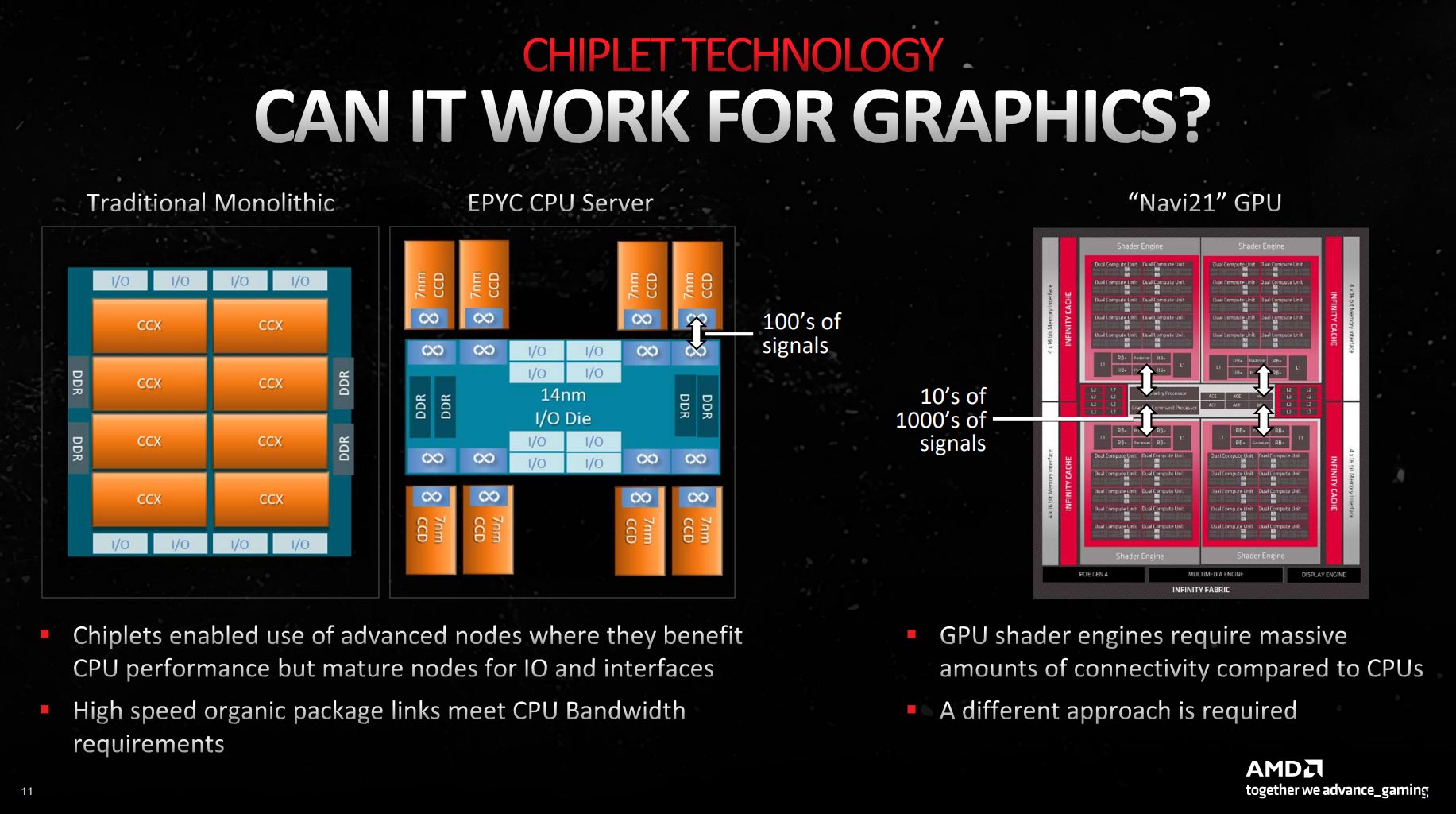
Jumping from a monolithic CPU design to a chiplet-based approach requires invention of high-speed, low-latency interconnects between what are termed Core Complex Dies (CCDs) and a central hub. That link is AMD-developed Infinity Fabric, which connects said chiplets with 100s of wires between dies.
A fantastic feat of engineering, AMD cannot take the same approach when looking at a chiplet-based GPU, and the reason has to do with the massive amounts of data traversing a GPU at any moment. Having upwards of 5,000 cores means the bandwidth required is an order of magnitude higher, and a standard Infinity Fabric approach simply cannot carry that amount of information in a design that has to sell for a set fee to make money.
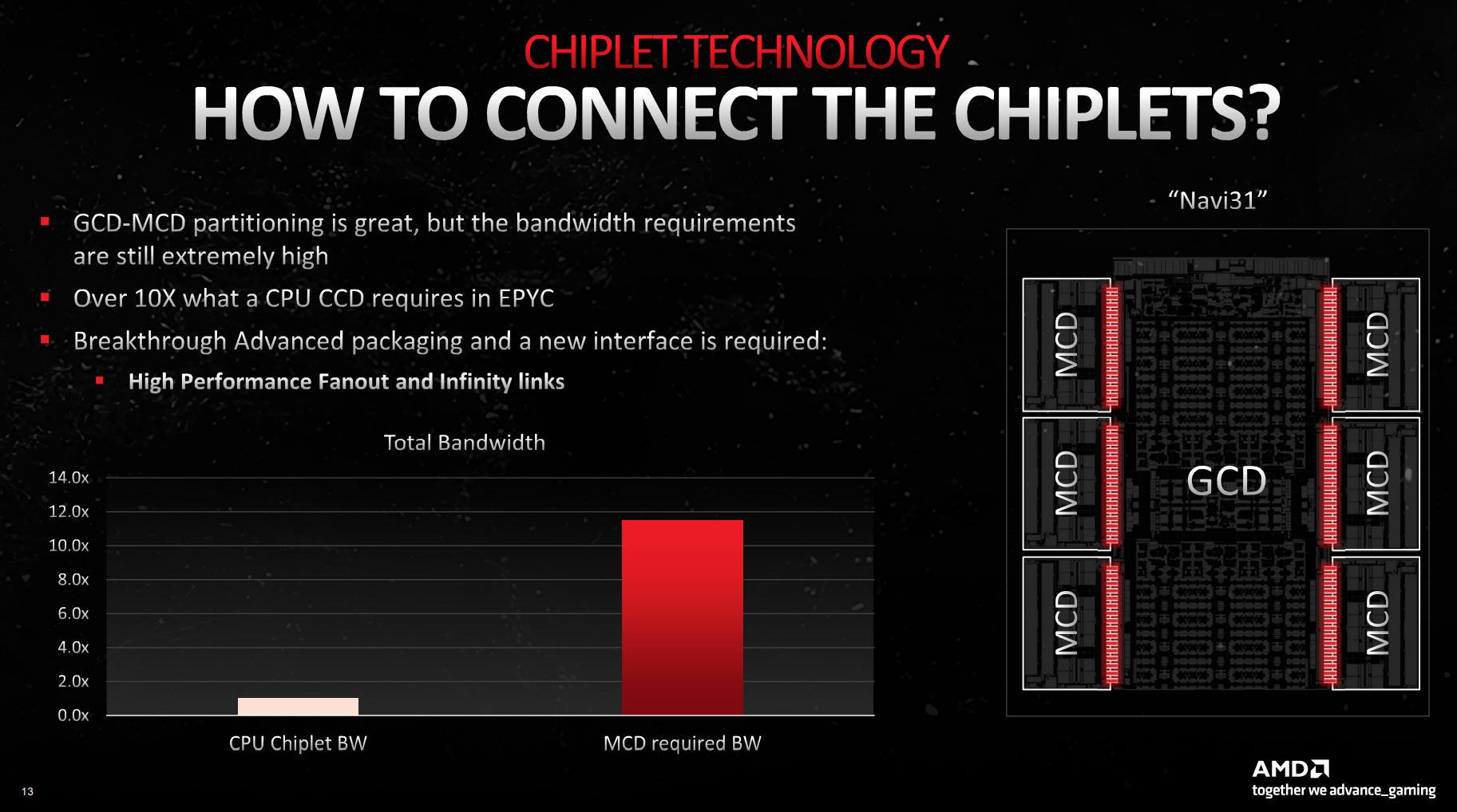
Putting this problem into intelligible context, AMD estimates a multi-chip GPU needs over 10x the bandwidth offered by the latest Epyc server processors. What to do and how to do it, eh? This is where smart engineering comes to the fore.
AMD’s approach is to flip the problem on its head, and by that we mean build a multi-core chip where the bandwidth-hungry memory partitions are manifested as smaller chiplets while the big computational engines are kept in a larger central die. If you recall, Ryzen processors do the reverse by moving cores to chiplets and memory to the IOD.
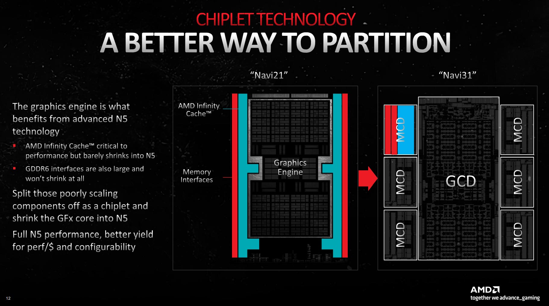
RDNA 3 is therefore built by having multiple Memory Cache Dies (MCDs), fabricated on a 6nm process, circling a larger, 5nm-based Graphics Core Die (GCD). Each MCD carries L3 cache and GDDR6 memory links to the GCD, and accumulating the contents of each MCD provides a good inkling of a card’s memory-side potential.
The GCD meanwhile, and just like Highlander there is only one, is home to familiar Compute Units (CUs) resident with shader cores, ray tracing cores, texture units, and the like.
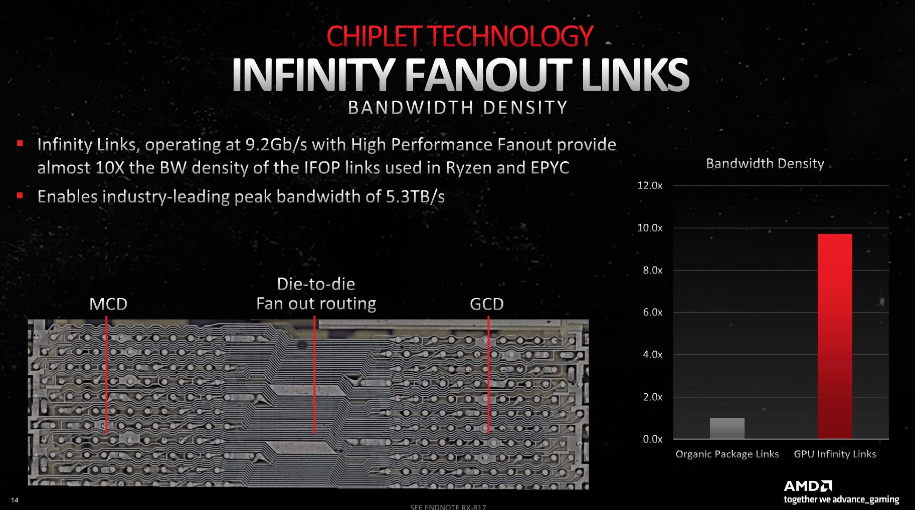
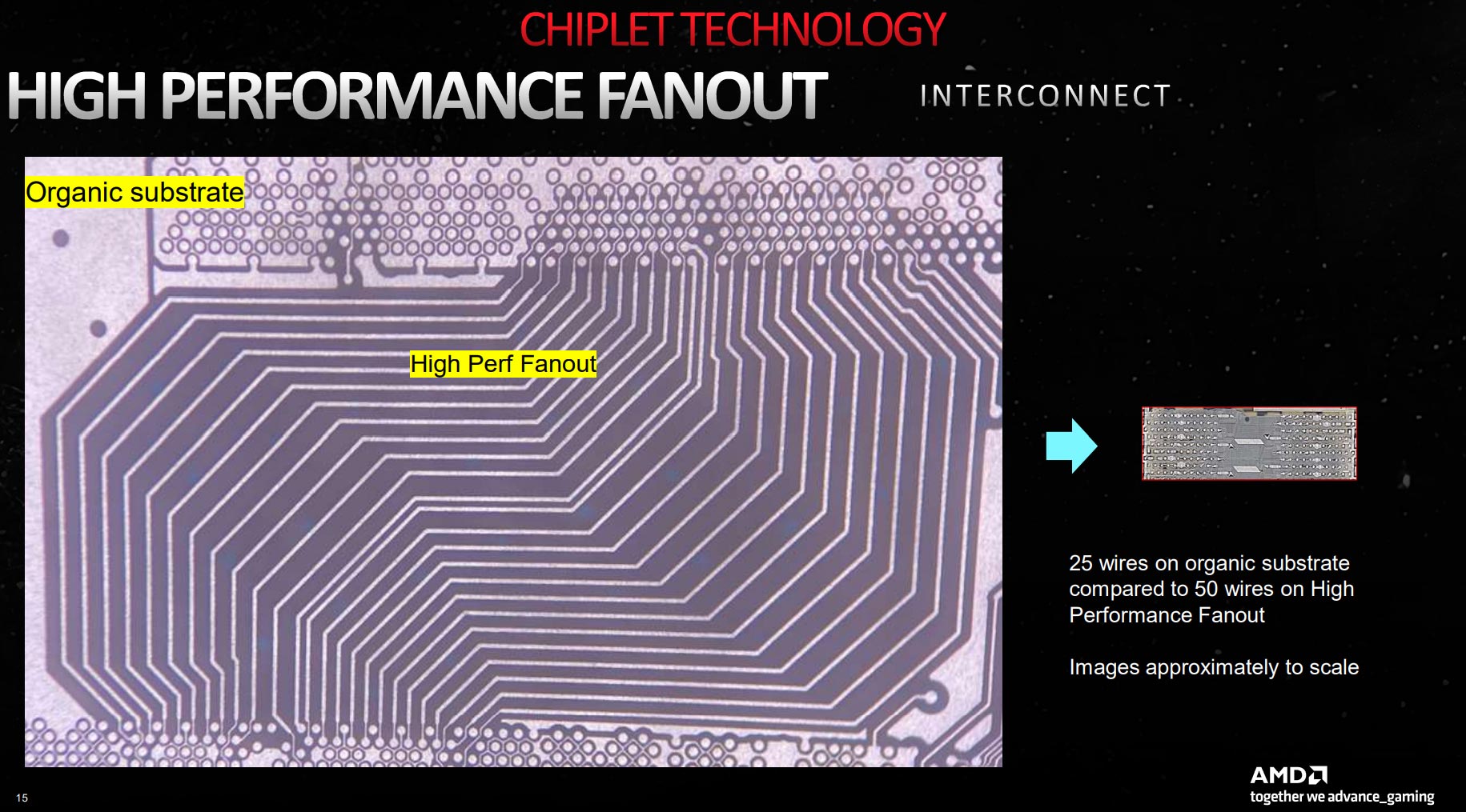
Linking MCDs to the GCD with the requisite bandwidth is the real triumph for RDNA 3. AMD calls this special sauce Infinity Fabric Fanout Technology (IFFT), illustrated in the slide above. Going by AMD’s presentations, each wire is far, far smaller than its CPU counterpart. If we crunch the numbers, GPU-optimised IFFT is over 50x as dense and provides 10x higher bandwidth than Infinity Fabric On Package (IFOP) used for CPUs. Take a moment for that to sink in.
We needed a new package technology and a new link technology. And that’s what we have implemented.
Sam Naffziger, AMD Senior Vice President and Product Technology Architect
Without IFFT, make no mistake, there is no chiplet-based RDNA 3, as scaling incumbent CPU IFOP technology would result in huge amounts of power diverted solely for the interconnects, let alone any die-space ramifications. Nevertheless, building links between chiplets isn’t a free energy lunch. IFFT takes crucial space and power to perform its high-speed data shuttles at 9.2Gb/s. We estimate adding relevant links, as opposed to a purely monolithic design, increases die area by close to 15 per cent while adding precious watts to overall consumption.
As it is, each TSMC-fabricated 6nm MCD weighs in at around 37mm² and houses some 2bn transistors. That’s a combined 222mm² and 12bn transistors right there for Navi 31 silicon. CU-housing GCD is a significant 300mm², meaning the combined size of the Navi multi-chip GPU is 522mm².
An interesting question arises. Is it better to have a 5nm monolith chip at 450mm² – the size we estimate Navi 31 would be on a single piece of silicon; there would be no space- and power-taking IFFT links – or a multi-chip 5nm/6nm at 522mm²? Not an easy one to answer, and one we’re sure AMD’s bean counters wrestled with.
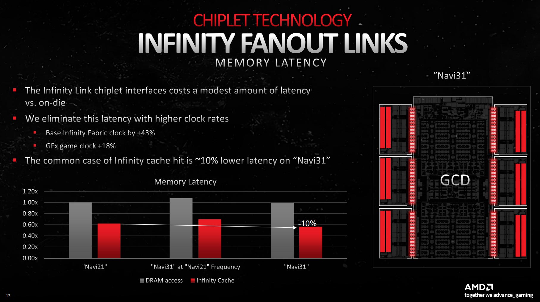
Another problem facing an IFFT solution is, on paper, one of latency. AMD acknowledges running Infinity Links will always create more latency than conducting transfers within one monolithic die. This issue is shown by the Navi 31 bars marginally higher than Navi 21. However, the combination of a 43 per cent higher IF clock and higher game clock ameliorates the issue. In fact, AMD contends Navi 31 has lower latency… but how much lower could it have been on a monolithic design?
We come away from the chiplet discussion with the thinking that AMD has spent a lot of time and resource in mitigating obvious issues emanating from going down a multi-chip route on a GPU. The pain is worth the long-term benefits, according to AMD, but it seems like a lot of effort.
The chiplet approach ought to play dividends further down the line when we have, say, 12 MCDs surround one or two GCDs. Breaking down the parts into manageable chunks, with presumably better yields than a monolithic monster, is where AMD is aiming. Whether it’s chiplets or tiles, we can foresee Nvidia adopt a similar approach in years to come.
RDNA 3 – Efficiency At The Core
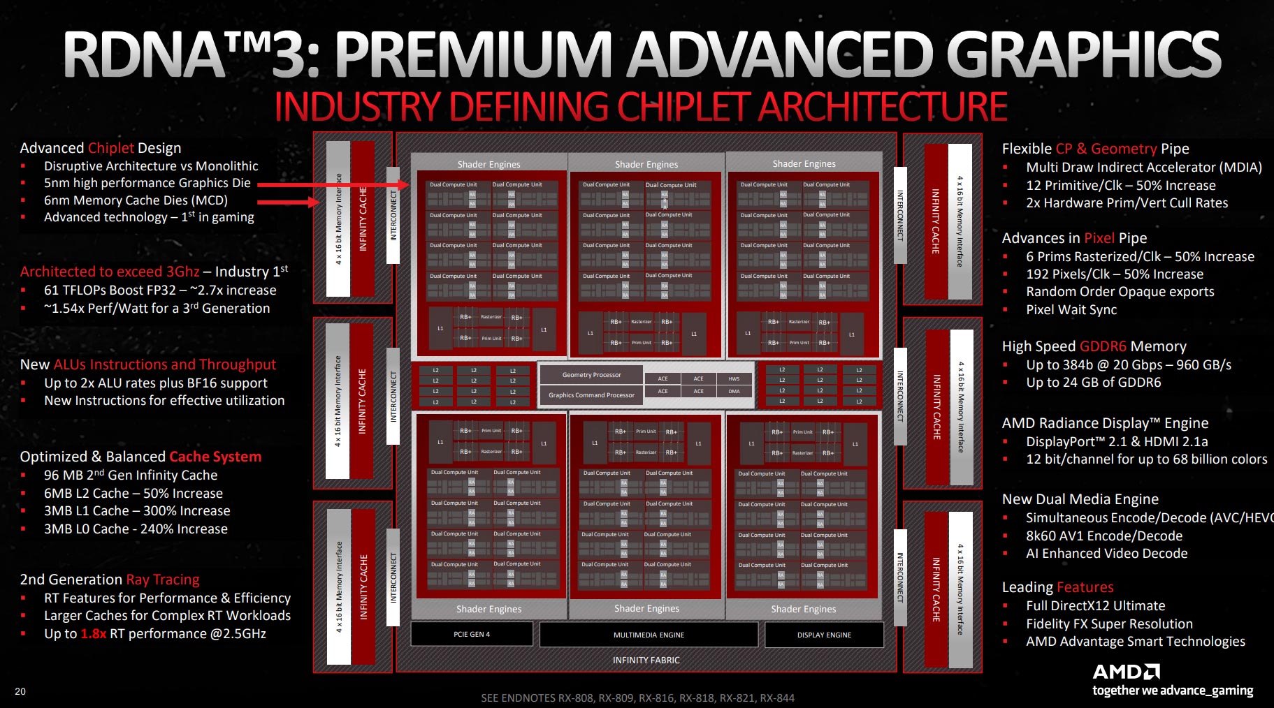
Feast your eyes on that, will you? Having marked off the first part of our discussion, as it pertains to a chiplet design and the whys and wherefores of going down that road, the second is RDNA 3 architecture.
Compared to Navi 21, AMD claims a 54 per cent performance-per-watt increase
It’s hard to miss AMD’s claims of RDNA 3 ‘architected to exceed 3GHz.’ This certainly isn’t the case in the first two cards based on this design, namely Radeon RX 7900 XTX and XT, suggesting AMD hasn’t achieved lofty frequency aspirations in the first retail salvo. A misjudgement of the architecture or relatively poor frequency yields from foundry partner TSMC? Probably a bit of both.
Nevertheless, there is positive news. Compared to Navi 21, which you’ll know as high-end Radeon RX 6000 Series, AMD claims a 54 per cent performance-per-watt increase. That’s nothing to be sniffed at, of course, and the rest of our discussion focusses on how AMD has achieved this number.
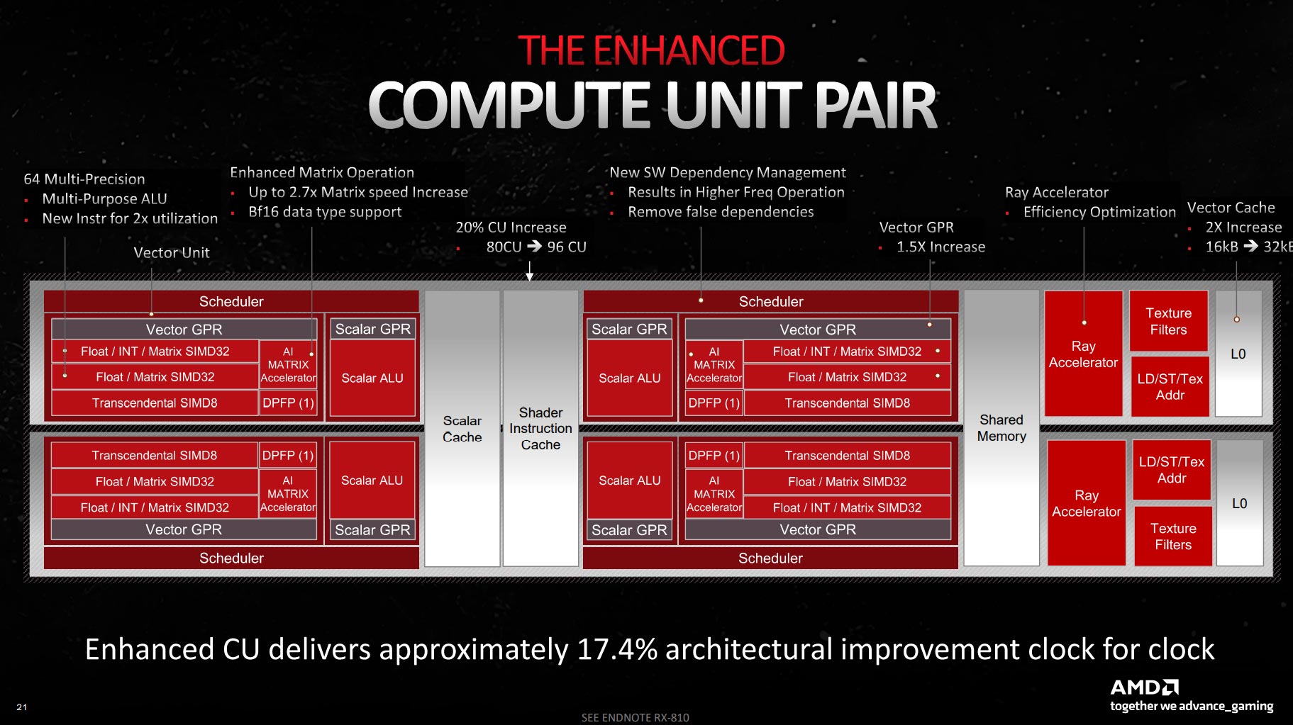
Performance naturally goes up for Navi 31 as it fits in more Compute Units than its immediate predecessor, and the 80CU-96-CU notation gives a 20 per cent boost right off the bat. Shoving in more CUs is entirely expected when moving between architectures and processes. Low-hanging fruit and all that.
Yet the devil is very much in the details. Take another look at the two CU blocks, or pairs. AMD refers to it as a single CU, of which, if you recall, there are 96 in the Big Boy design. But it’s not one CU, is it, as the second is a mirror of the first.
This has important ramifications for performance, and why comparing generation-on-generation is fast bordering on pointless. AMD has effectively doubled each CU’s ALU capability – initialisms, ahoy – meaning there’s double the throughput for floating-point tasks on a shader-to-shader basis.
Breaking it down, each RDNA 3 64-ALU block, or CU, has twice as many FP32 pathways of RDNA 2. Here’s where terminology becomes difficult when referring to ALUs, FP32 units and INT32 units, but suffice to say, FP operations, which are a mainstay of gaming, are much improved.
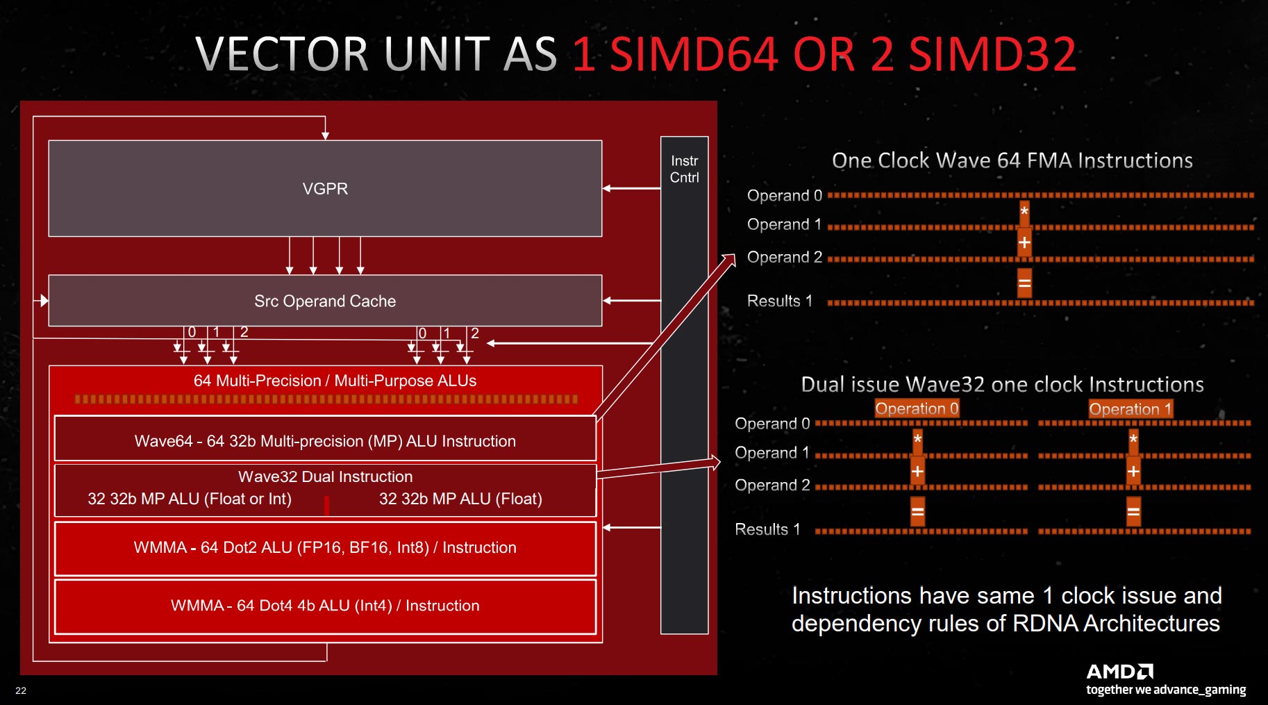
On the integer side, AMD has all-new AI Matrix Accelerators which include bfloat16 and WMMA64 Dot4 support, primarily to help with convolution, which is one of the fundamental operations of deep neural networks with demanding matrix computation. In other words, it is AMD’s answer to Nvidia’s Tensor Cores. Little more is known of the technology other than basic specs and a purported 2.7x matrix speed increase compared to RDNA 2.
Cache Me In
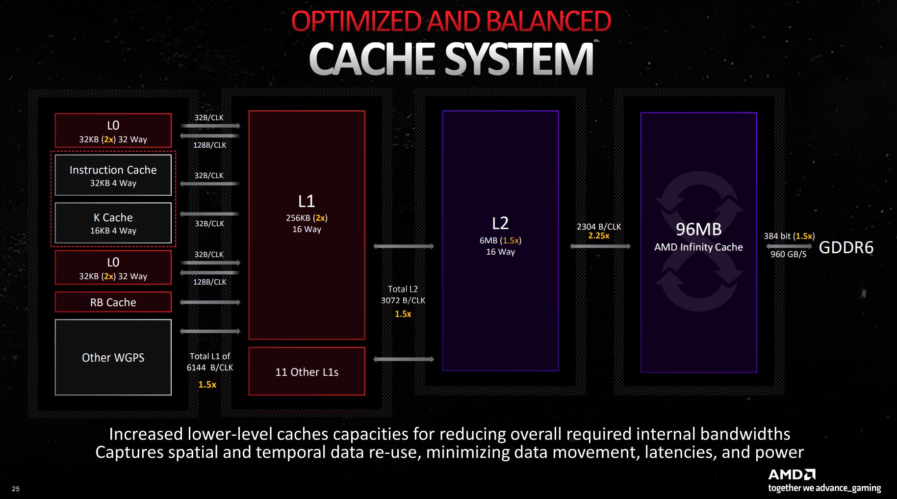
Having a more robust, faster core and memory subsystem helps, but most iterative GPU architectures tend to devote increasing amounts of space for larger caches. Just see what Nvidia did with RTX 40 Series.
Going through the information, it’s easy to see where AMD has doubled sizes compared to RDNA 2. Certainly not the massive increases instigated by Nvidia, yet it stands to reason that caches need to be upgraded to deal with more innate processing power.
The one outlier from this approach is AMD Infinity Cache. Those familiar with how AMD builds recent GPUs will know Radeons have a slab of goodly cache residing between on-chip L2 and external GDDR6. Call it an L3 if you will. RDNA 2’s Infinity Cache topped out at 128MB on Radeon RX 6950 XT. AMD drops it to 96MB for RDNA 3. If larger caches are better and there’s been plenty of increase on L0, L1, and L2, what gives? Good question.
It’s not the size, it’s how you use it, seems to be AMD’s response. Rather than scale this apparent L3 to 128MB+, which takes up valuable real-estate space, AMD has increased the conduit between L2 and Infinity Cache by 2.25x. That’s no small potatoes. Aforementioned RX 6950 XT runs off a 1,024 bytes per clock and has an SoC operating at 1.93GHz achieving total bandwidth of 2TB/s. Navi 31’s best SoC operates at 2.3GHz. Do the math and we reach 5.3TB/s at this juncture alone, without taking the much wider, faster GDDR6 into account.
In that regard, Navi 31 (RX 7900 XTX) has a maximum 384-bit memory bus feeding GDDR6 memory operating at 20Gbps, whereas Navi 21 (RX 6950 XT) is only 256 bits wide and 18Gbps. 576GB/s cannot compete with 960GB/s on today’s champ.
Ray Tracing Overhaul
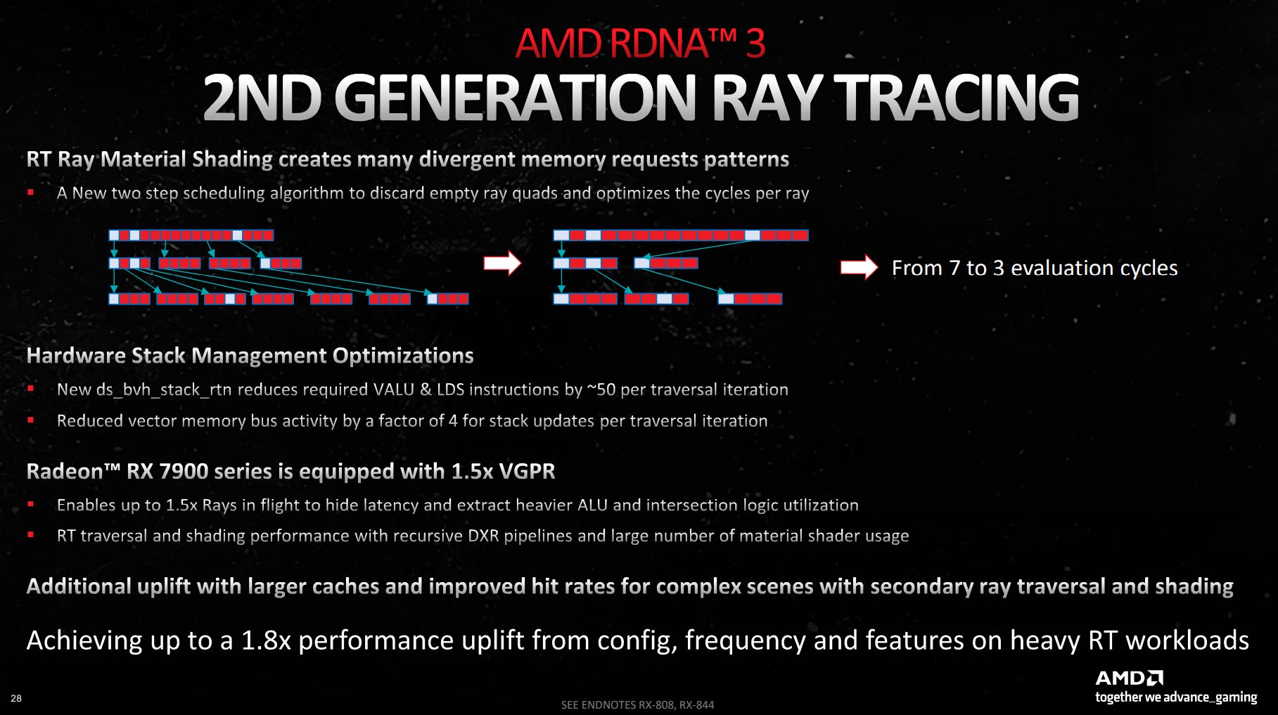
AMD introduced dedicated hardware ray tracing units in RDNA 2. Yet while rasterisation performance was roughly analogous to price-comparable Nvidia RTX 30 Series, RT lagged behind considerably. The gap has become a chasm with the introduction of RTX 40 Series, so if you want best-in-class lighting, Team Green is the way to go.
Looking to arrest this gulf, AMD has invigorated the RT units within RDNA 3. As RT hardware is tied to CUs on a one-to-one basis, there is more ray tracing potential through sheer numbers – 96 Ray Accelerators vs. 80.
we’d put the best-case RT scenario as one matching premium RTX 30 Series cards
AMD’s focus on RDNA 3 isn’t an entirely new RT unit – that would be too costly to implement at this stage – but one of improving what it has to work with. Part of this rests with efficiency, insofar as not doing work that’s of no use. RDNA 3 introduces an early subtree culling to remove unnecessary calculations by skipping parts of the acceleration structure during traversal.
There are further improvements, too, from having more rays in flight to natural uplifts caused by larger caches, CUs, and so forth, but the bottom line is that combined efforts are no silver bullet; we’re not going to see Nvidia RTX-like numbers anytime soon. In fact, though AMD contends an 80 per cent improvement for RDNA 3 over RDNA 2, we’d put the best-case RT scenario as one matching premium RTX 30 Series cards. RTX 40 Series will remain in a different league.
Bits And Bobs
Head back up and look across to the advancements in the pixel pipe. Complementing the increased top-end muscle, AMD ups ROP count by 50 per cent, from 128 to 192.
We touched on bandwidth hikes earlier, yet it’s prudent to recap. AMD’s Infinity Cache is 165 per cent faster and external memory affords 67 per cent over the previous generation. You gotta feed the CU beast.
On the display side of things, AMD keeps to HDMI 2.1a of the previous generation and adds in DisplayPort 2.1, which is a feature missing on rival Nvidia RTX 40 Series cards.
A Dual Media Engine brings hardware-accelerated support for AV1 encode and decode up to 8K60, among other niceties, and outputs are such that a single card can drive four 4K144 displays.
Enter Radeon RX 7900 XTX and XT
| Radeon | RX 7900 XTX | RX 7900 XT | RX 6950 XT | RX 6800 XT |
|---|---|---|---|---|
| Launch date | Dec 2022 | Dec 2022 | May 2022 | Nov 2020 |
| Codename | Navi 31 | Navi 31 | Navi 21 | Navi 21 |
| Architecture | RDNA 3 | RDNA 3 | RDNA 2 | RDNA 2 |
| Process (nm) | 5/6 | 5/6 | 7 | 7 |
| Transistors (bn) | 57.7 | 57.7 | 26.8 | 26.8 |
| Die size (mm2) | 522 | 522 | 520 | 520 |
| Compute Units | 96 of 96 | 84 of 96 | 80 of 80 | 72 of 80 |
| ALUs | 6,144 | 5,376 | 5,120 | 4,608 |
| Boost clock (MHz) | 2,500 | 2,400 | 2,310 | 2,250 |
| Peak FP32 TFLOPS | 61.44 | 51.61 | 23.65 | 20.74 |
| RT cores | 96 | 84 | 80 | 72 |
| AI cores | 192 | 168 | – | – |
| ROPs | 192 | 192 | 128 | 128 |
| Infinity Cache (MB) | 96 | 80 | 128 | 128 |
| Memory size (GB) | 24 | 20 | 16 | 16 |
| Memory type | GDDR6 | GDDR6 | GDDR6 | GDDR6X |
| Memory bus (bits) | 384 | 320 | 256 | 256 |
| Memory clock (Gbps) | 20 | 20 | 18 | 16 |
| Bandwidth (GB/s) | 960 | 800 | 576 | 512 |
| Power (watts) | 355 | 315 | 335 | 300 |
| Launch MSRP ($) | 999 | 899 | 1,099 | 649 |
All of our discussion has rightfully centred on the overarching RDNA 3 architecture and consequent Navi 31 GPU. Both terms describe the available hardware tools from which AMD constructs retail cards. Those are Radeon RX 7900 XTX and Radeon RX 7900 XT, both hewn from Navi 31, albeit differently.
Starting with the best Radeon to date, RX 7900 XTX uses the full 96-CU complement available on the die – there is no holding back, unlike how Nvidia traditionally keeps cores unused on consumer graphics cards. It’s a big beast, alright, with 57.7bn transistors spread over the six MCDs and GCD. Simple math informs us 12bn of those go towards the former and 45bn to the cores.
Depending on how one defines ALUs RX 7900 XTX has either 6,144 (how we prefer to understand it) or 12,288, as each pair is capable of floating-point operations. It doesn’t matter, actually, as peak TFLOPS is the same no matter which side of the ALU fence you sit on.
61.44TFLOPS is exactly 10 billion times larger than the traditional ALU count. We arrive at this figure by multiplying the peak boost clock of 2,500MHz by the operations per clock, which in this case is four. Viewed on paper alone, RX 7900 XTX batters RX 6950 XT – the best of the last generation – into submission through massive firepower.
Making matters more confusing, AMD decouples the front-end clock from the shader clock. The reason to do so rests with saving power on the cores by running them more slowly, though with a boost clock of 2,500MHz, both shader and front-end clocks become synced again.
Right-o, let’s get to what you’ve been waiting for.
Performance
Our 5950X Test PCs
Club386 carefully chooses each component in a test bench to best suit the review at hand. When you view our benchmarks, you’re not just getting an opinion, but the results of rigorous testing carried out using hardware we trust.
Shop Club386 test platform components:
CPU: AMD Ryzen 9 5950X
Motherboard: Asus ROG X570 Crosshair VIII Formula
Cooler: Corsair Hydro Series H150i Pro RGB
Memory: 32GB G.Skill Trident Z Neo DDR4
Storage: 2TB Corsair MP600 SSD
PSU: be quiet! Straight Power 11 Platinum 1300W
Chassis: Fractal Design Define 7 Clear TG
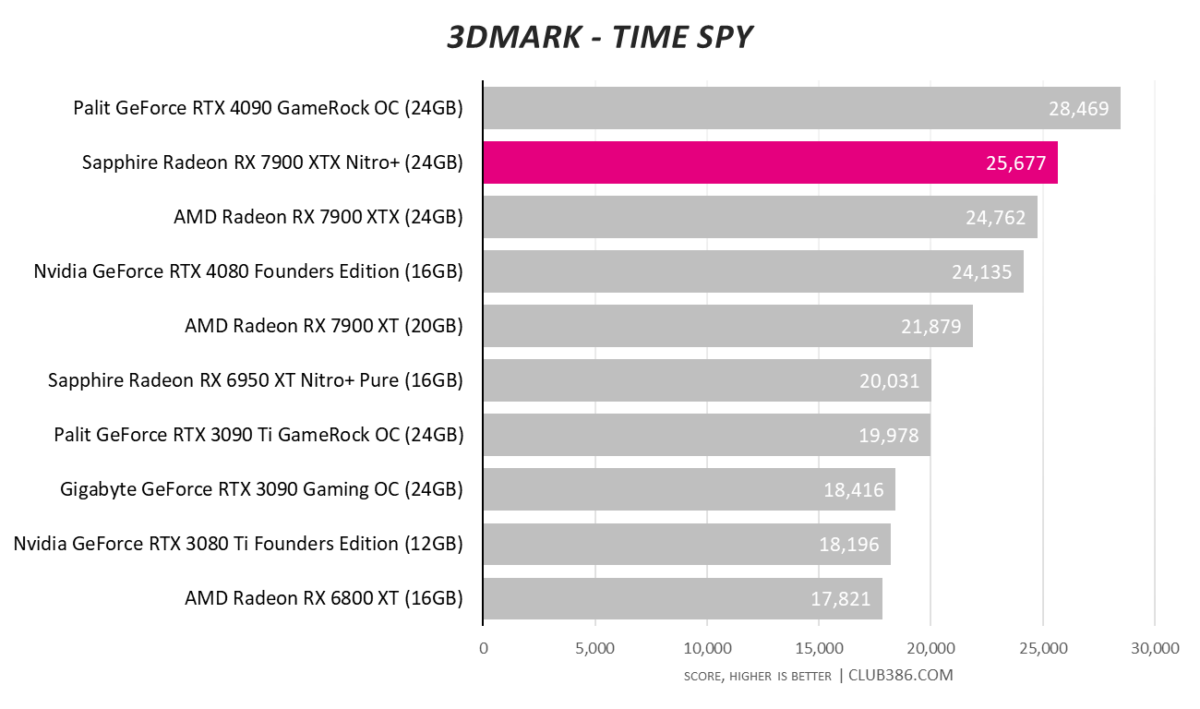
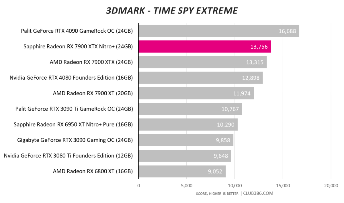
Our logs show the Sapphire Nitro+ averages 2,794MHz during benchmarks, albeit with memory at stock speeds, naturally elevating performance above the MBA card by a discernible degree.
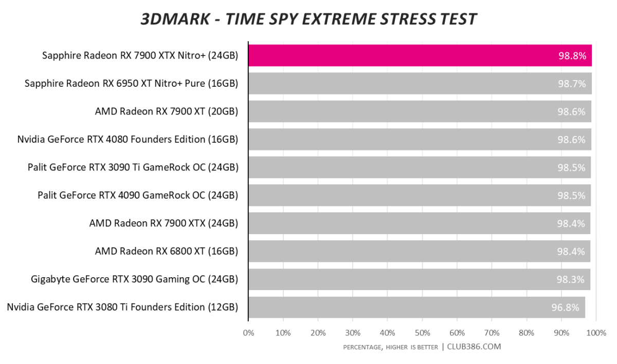
Massive heatsink meets 420W GPU. The winner, ladies and gentlemen, is Sapphire’s triple-slot cooling.
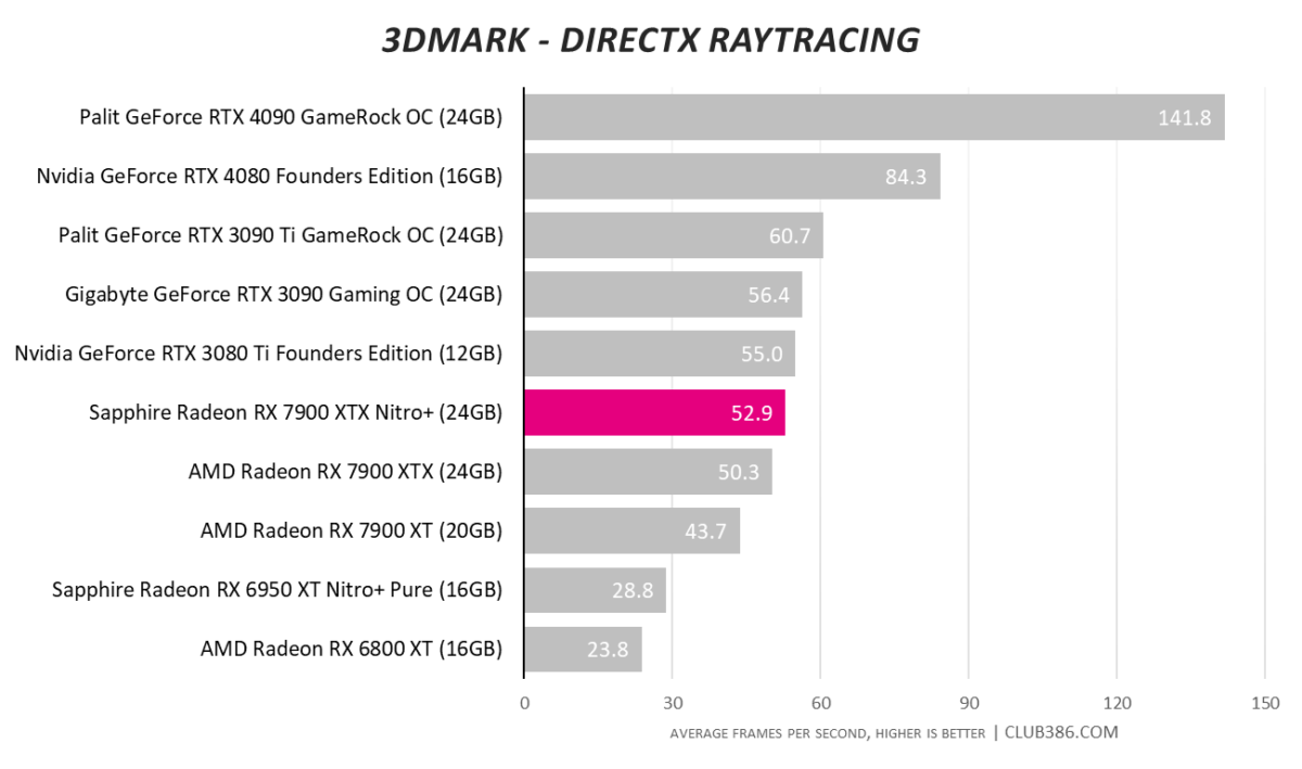
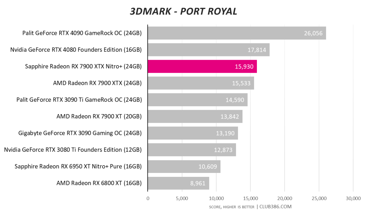
Raytracing numbers are improved from the last generation, of course, yet Nvdia’s peerless RTX 4090 is on a different level.
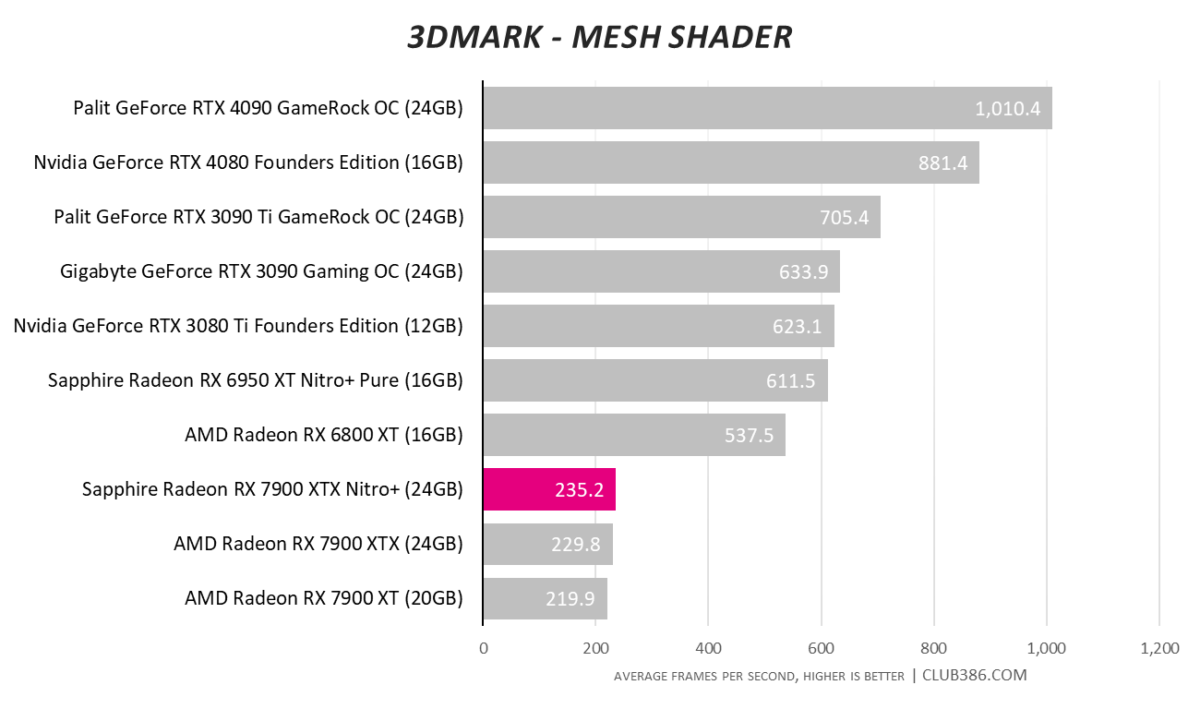
There’s been plenty of discussion whether the mesh shader operation on Navi 31 isn’t working correctly. Futuremark’s numbers think so – even with the latest updates – and we have reached out to AMD for comment.
Assassin’s Creed Valhalla
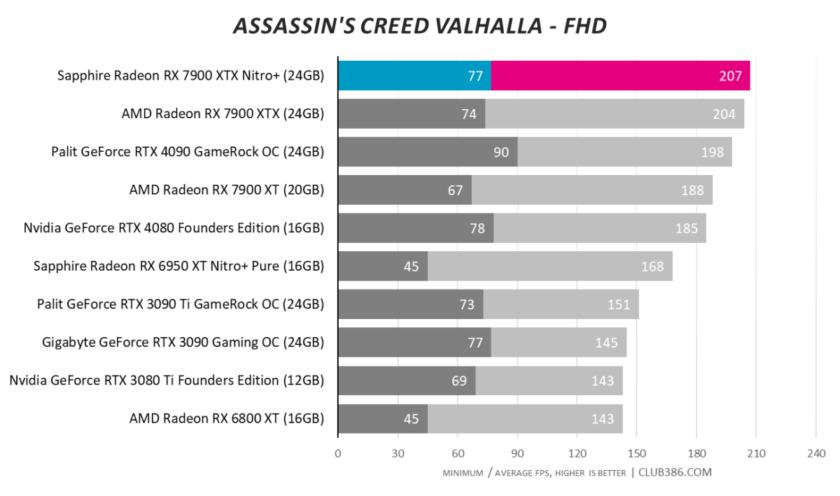
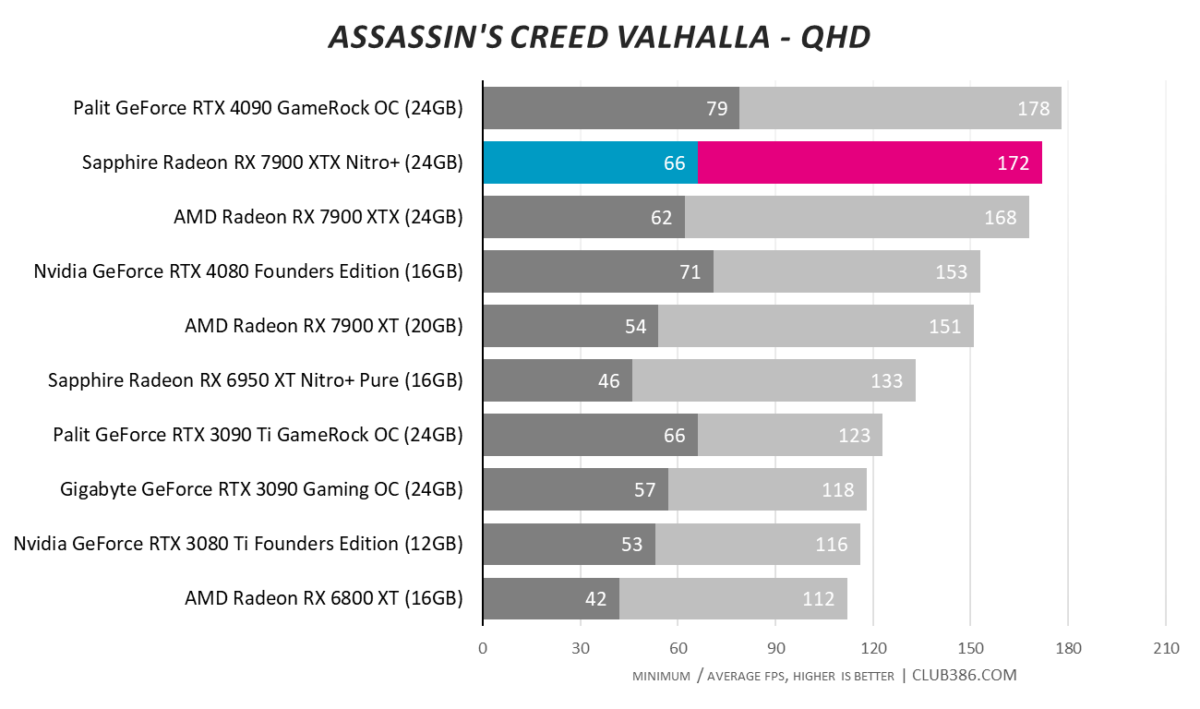
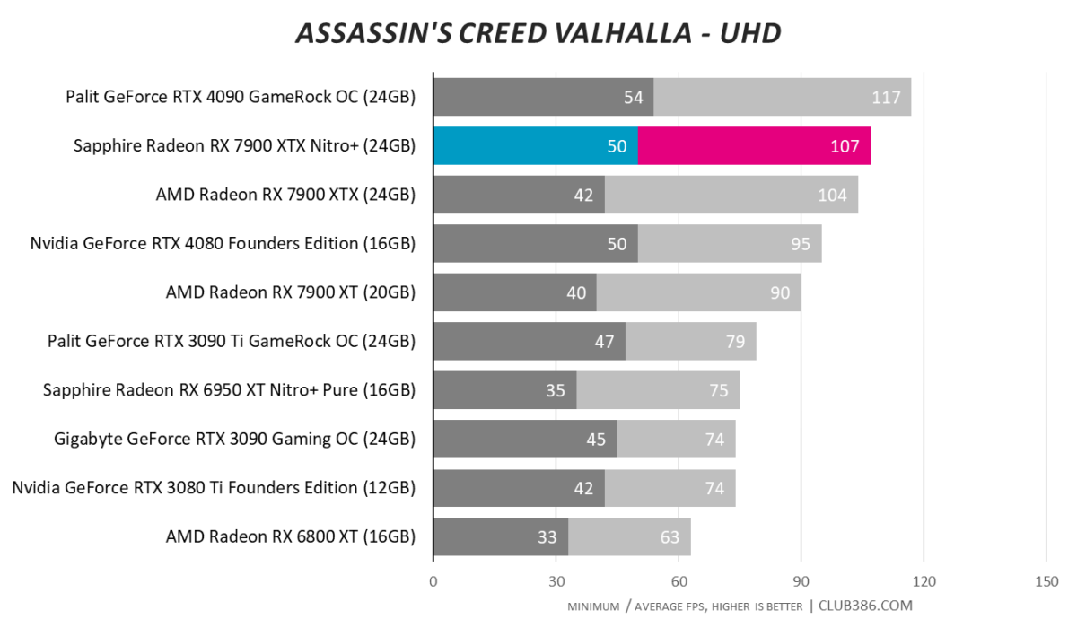
4K100 with ease? No problem for Sapphire’s best-ever card.
Cyberpunk 2077
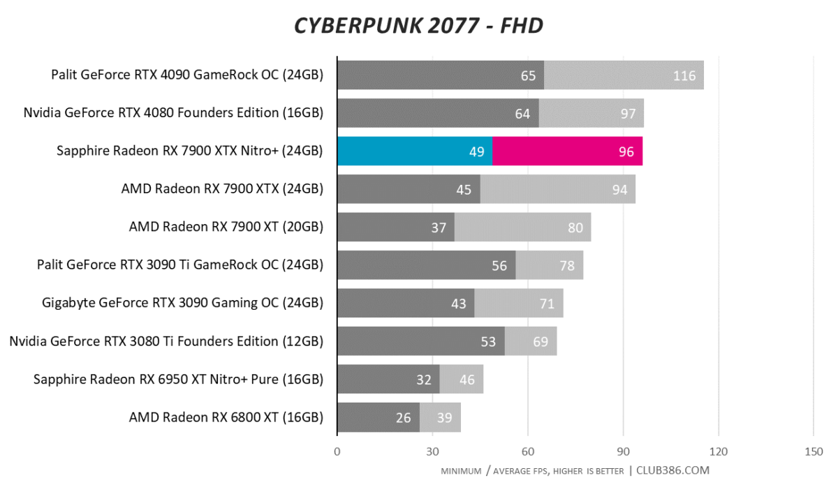
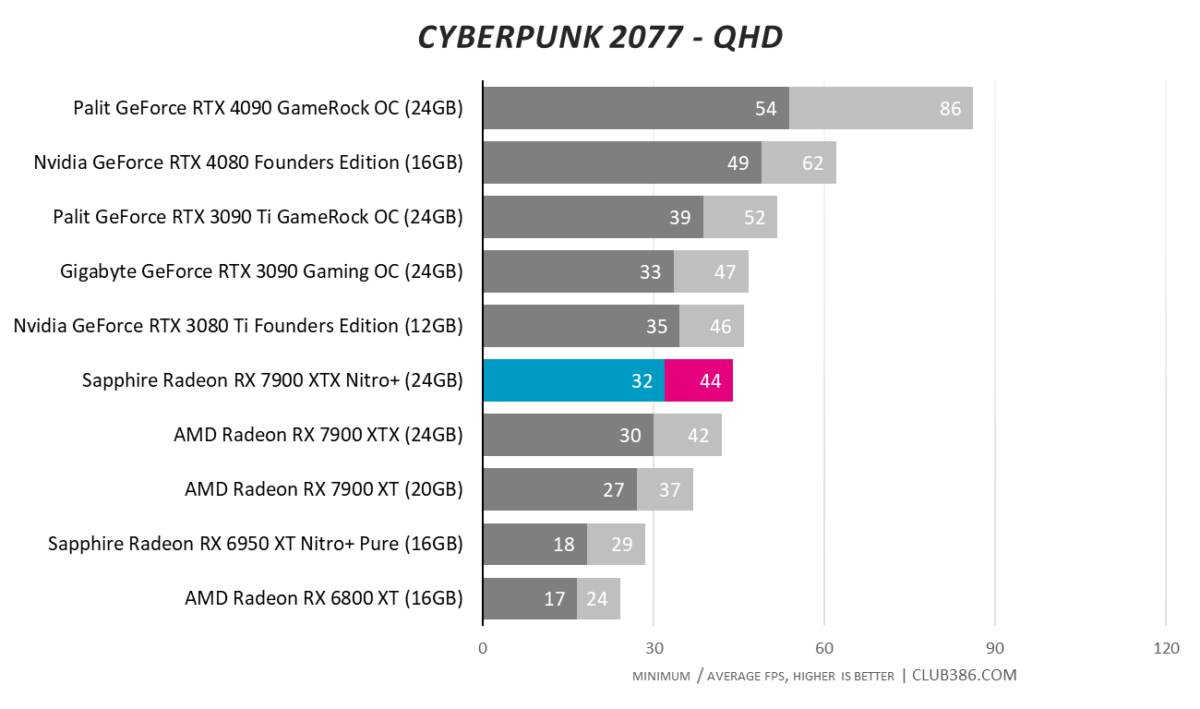
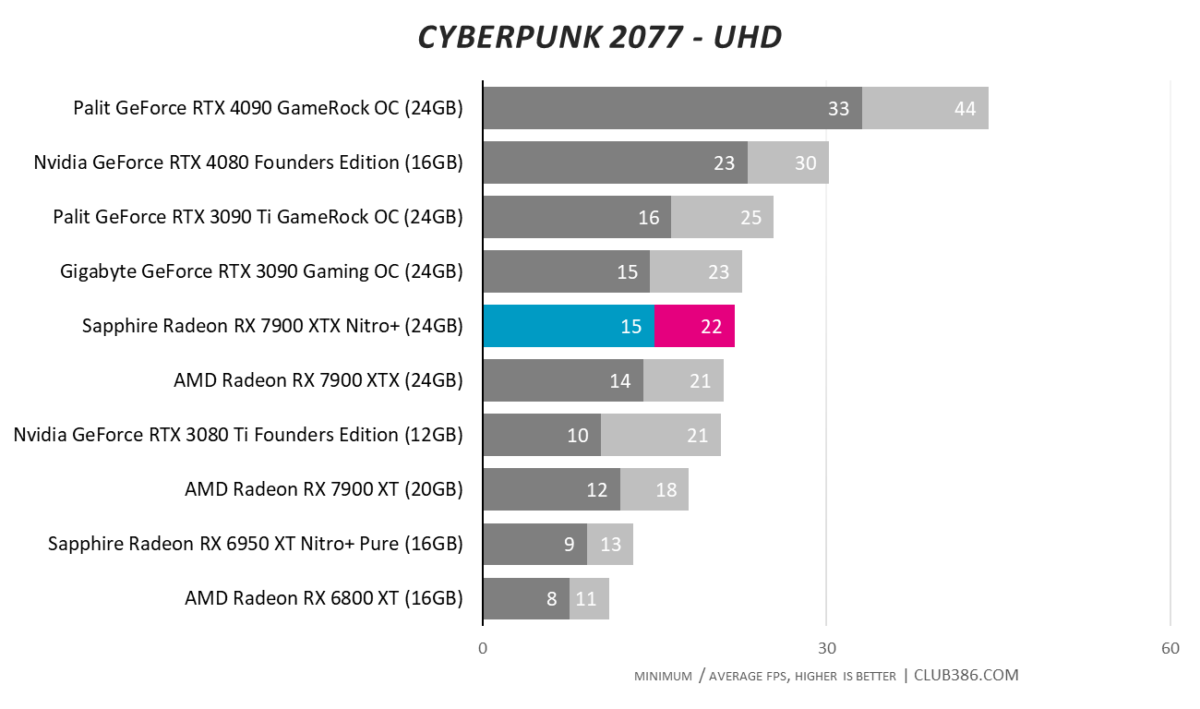
The spectre of substandard raytracing performance continues to haunt AMD. Not able to match the best of Nvidia’s last-generation cards, RTX poster child, Cyberpunk 2077, needs additional frame-boosting technology to hit 60fps at a QHD resolution.
Far Cry 6
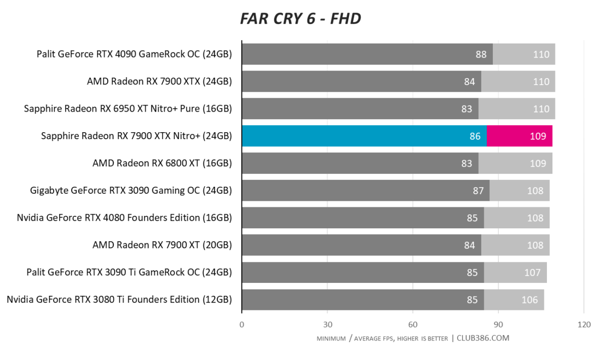
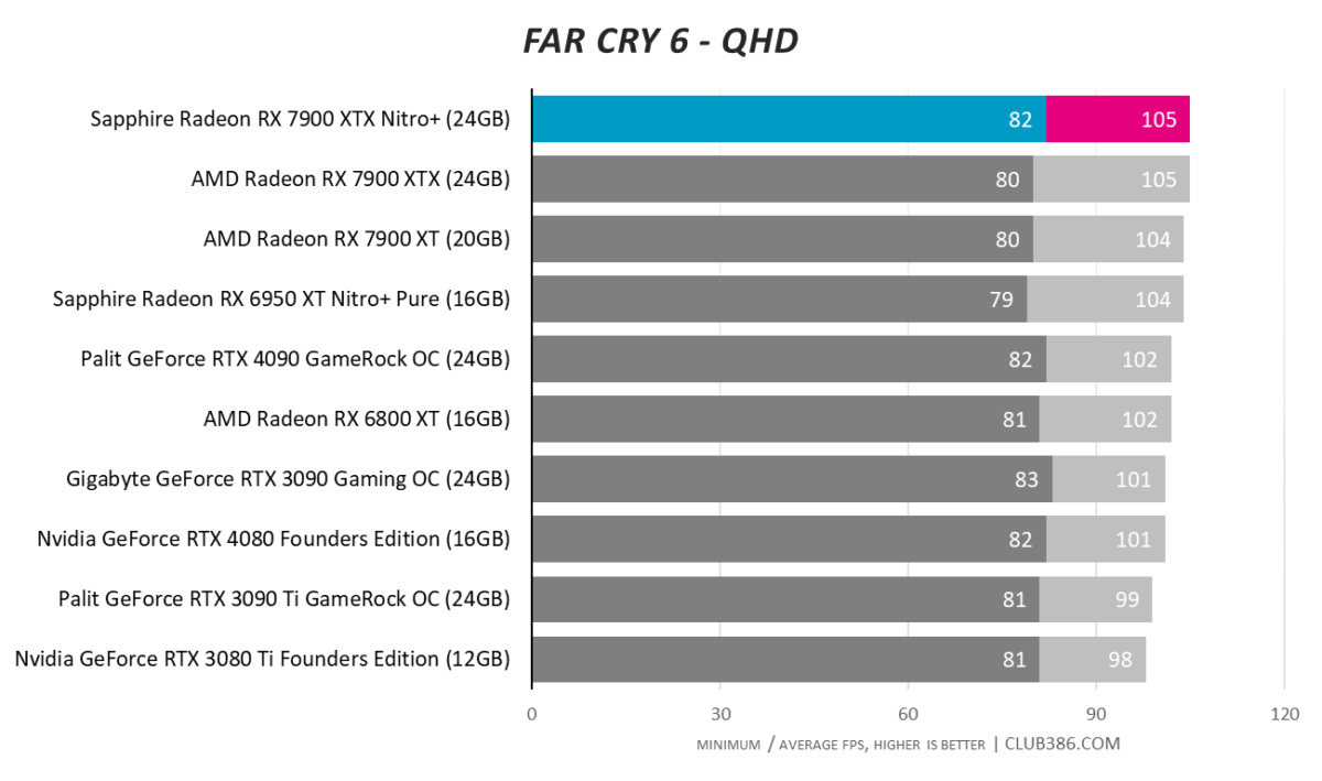
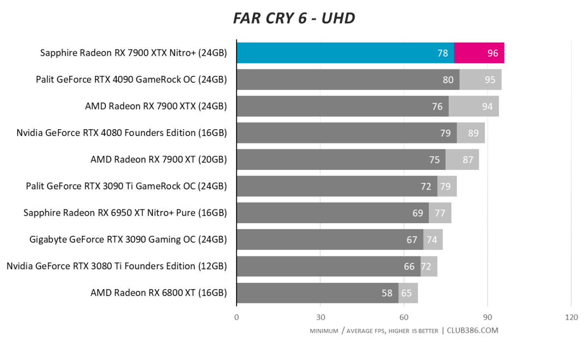
A high-quality RX 7900 XTX is able to squeak past a far dearer RTX 4090 in this title. Food for thought.
Final Fantasy XIV: Endwalker
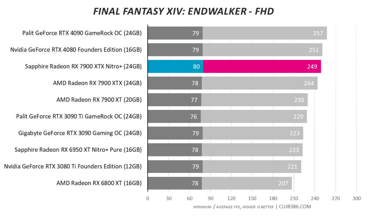
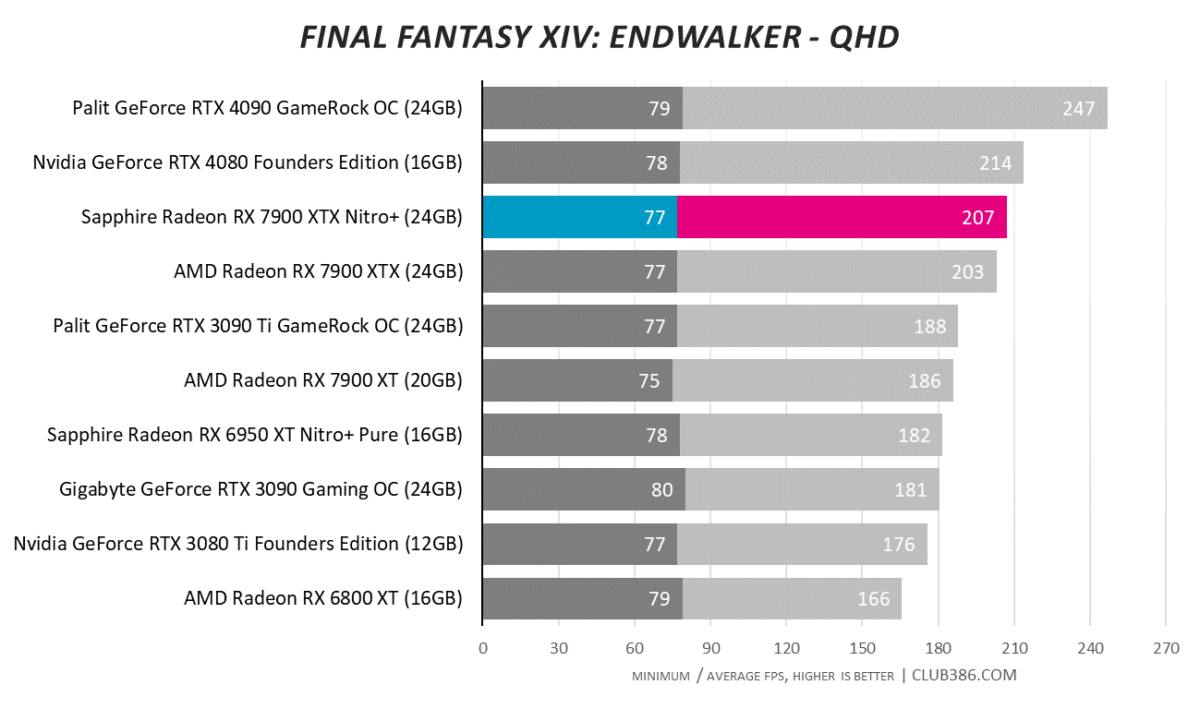
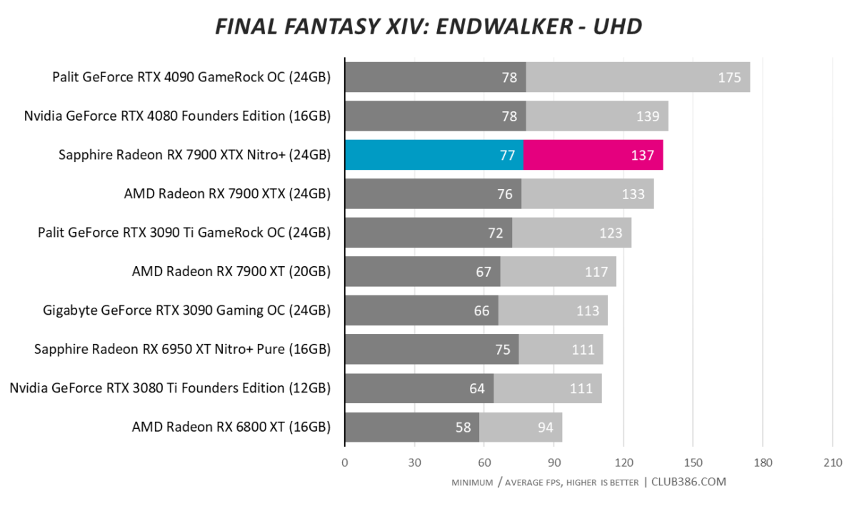
One ought to expect excellent framerates in older games. 4K100 is a breeze in Final Fantasy XIV: Endwalker.
Forza Horizon 5
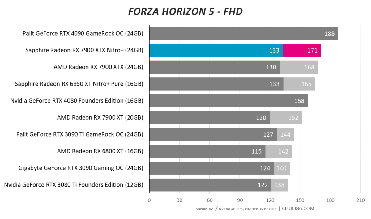
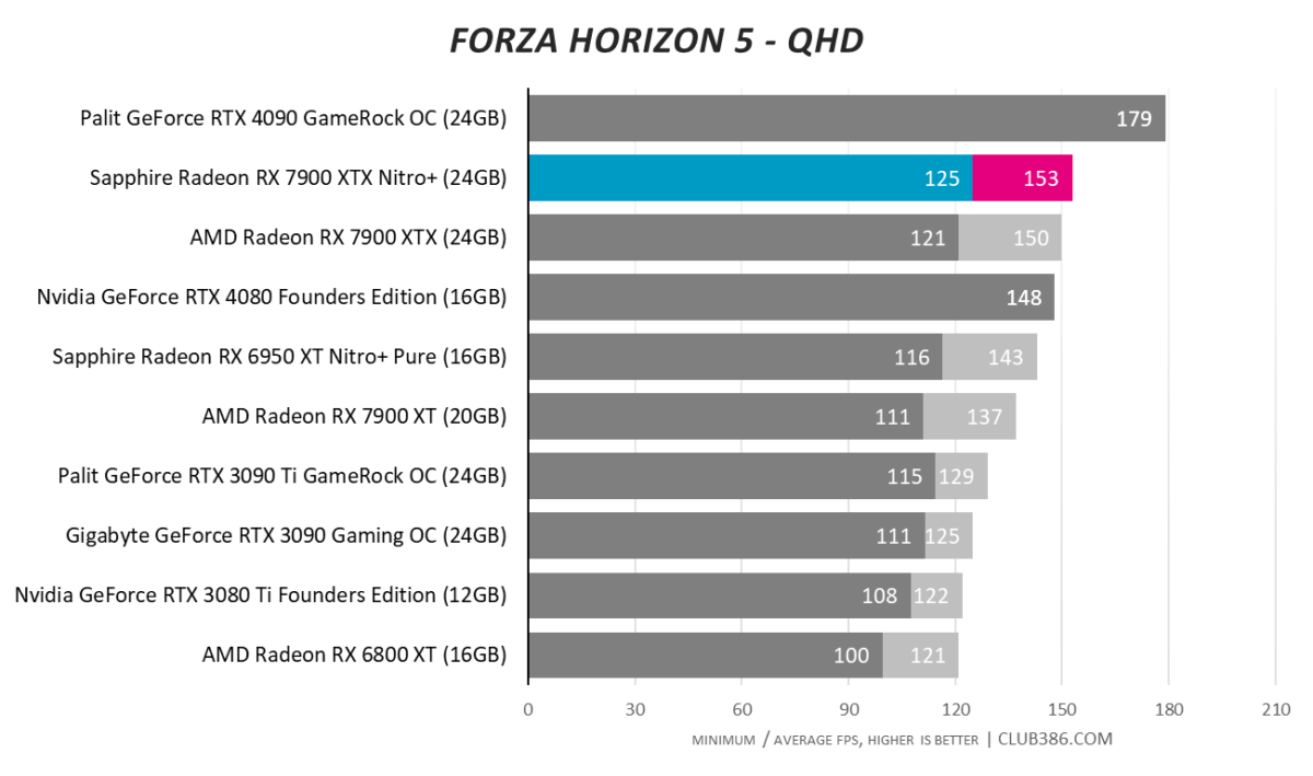
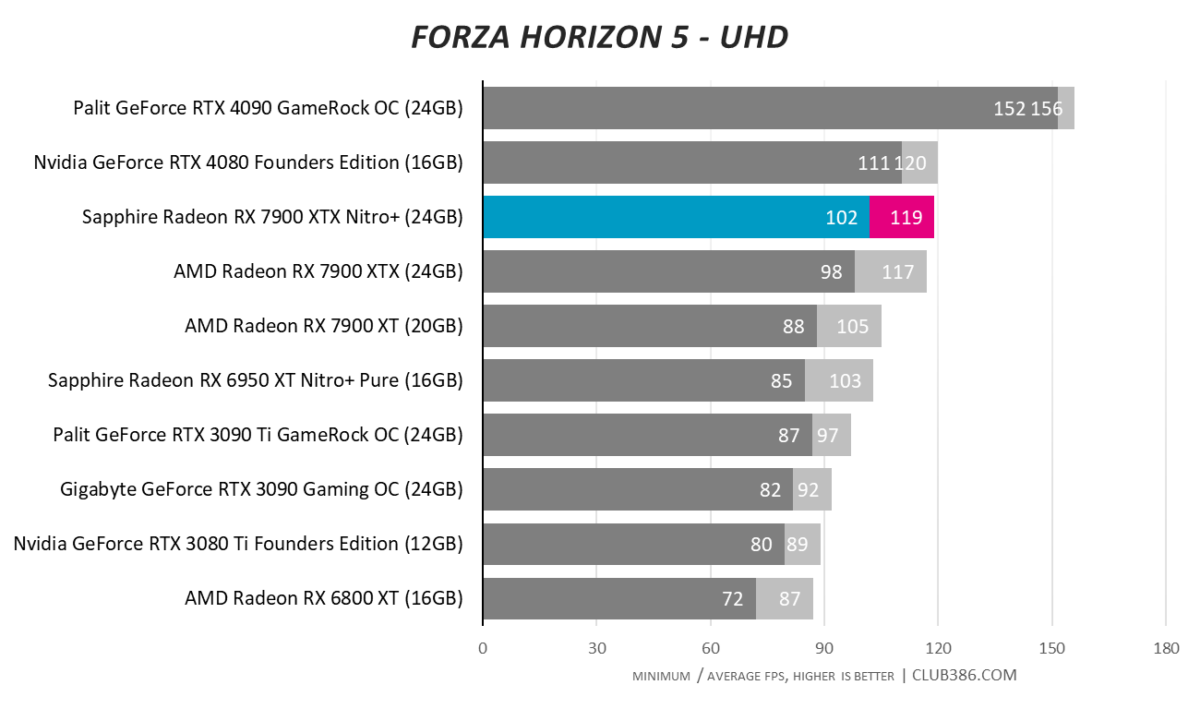
Another game, another 4K100-busting benchmark score. Radeon RX 7900 XTX really is a premium GPU; Sapphire adds the icing on top.
Marvel’s Guardians Of The Galaxy
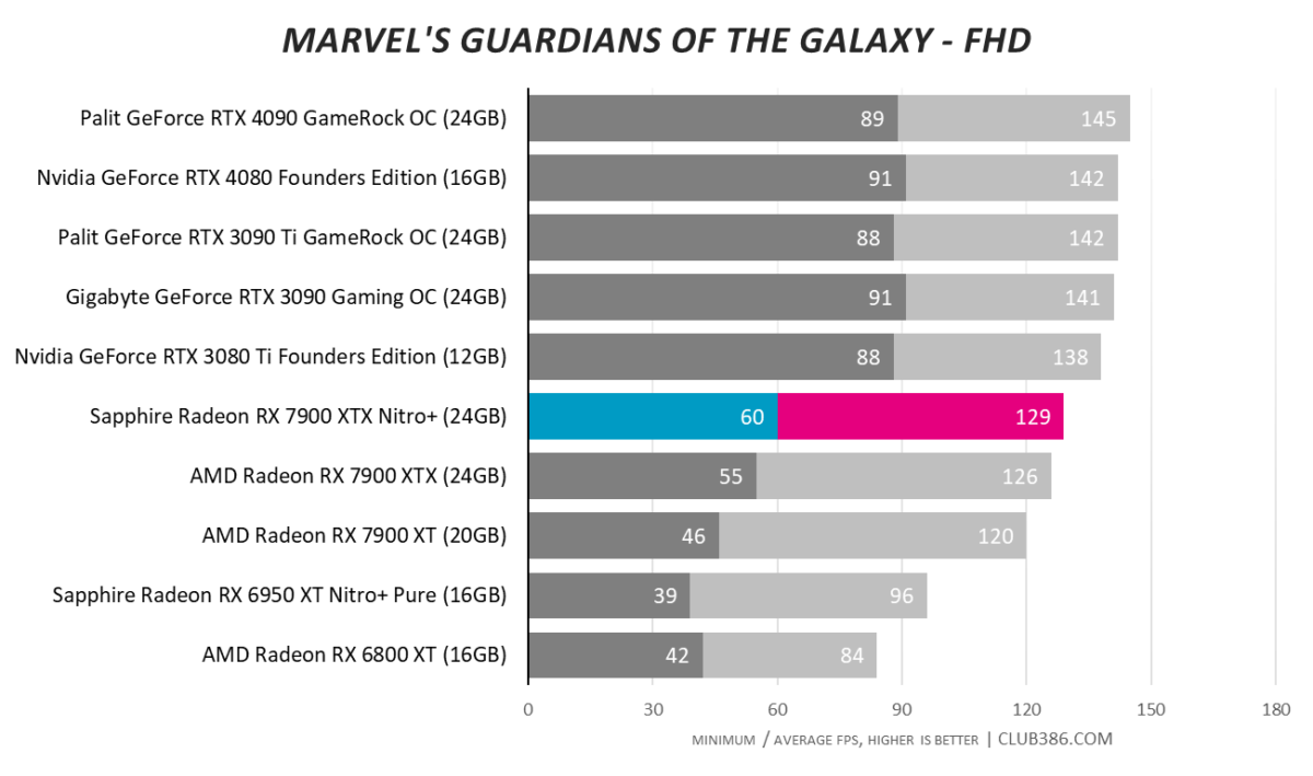
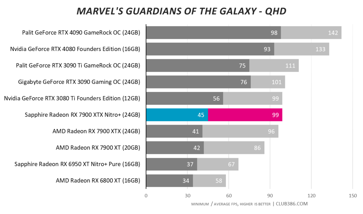
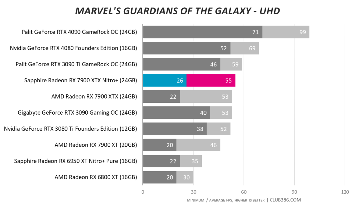
The raytracing Achilles heel is in evidence when run in the most taxing mode.
Tom Clancy’s Rainbow Six Extraction
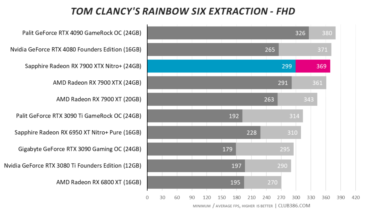
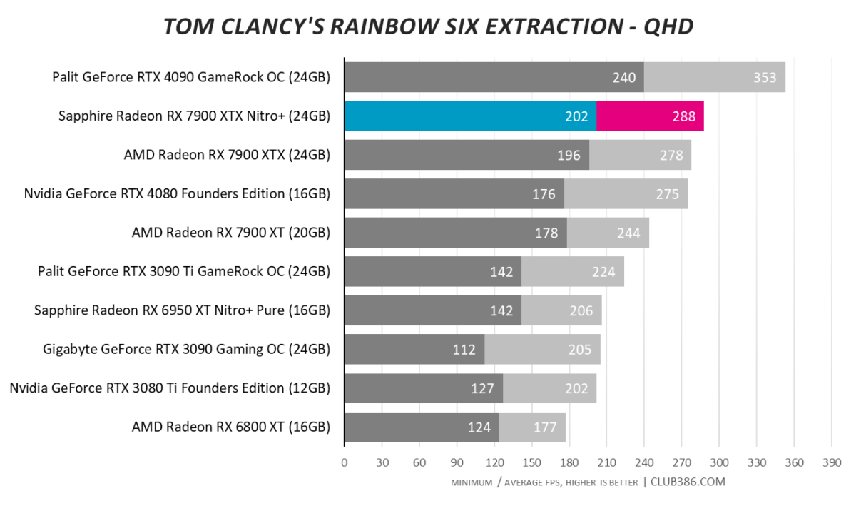
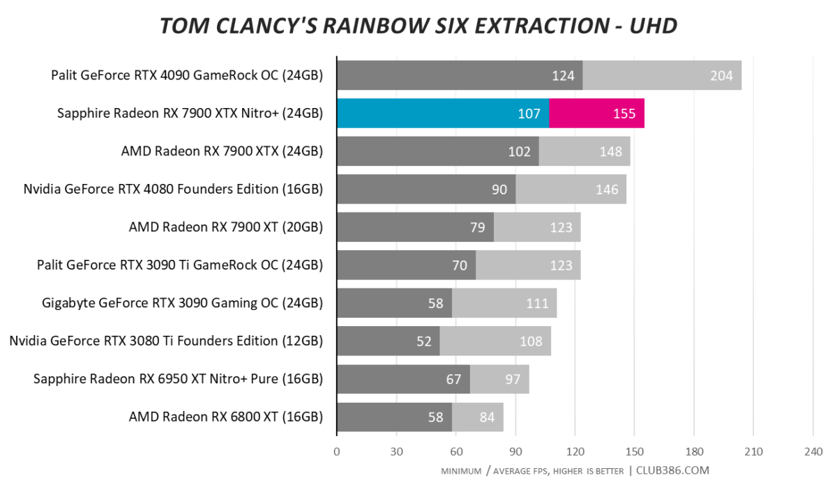
Radeon RX 7900 XTX is an excellent card for games relying on rasterisation to paint pixels. Adding raytracing to the mix pushes recommendations towards GeForce.
Vitals
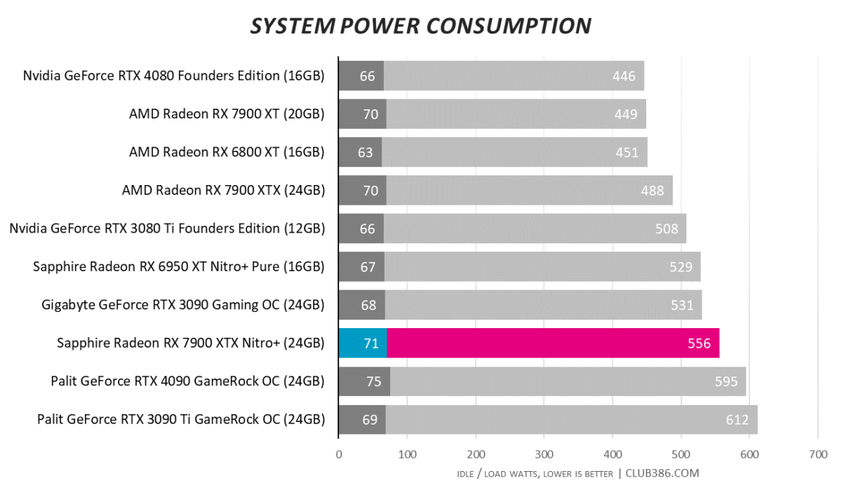
Equipped with 420W board power, required to run the higher clocks, causes system-wide power consumption to rise by a significant amount over the MBA card. Nevertheless, there’s no need to go hunting for a 1,500W PSU.
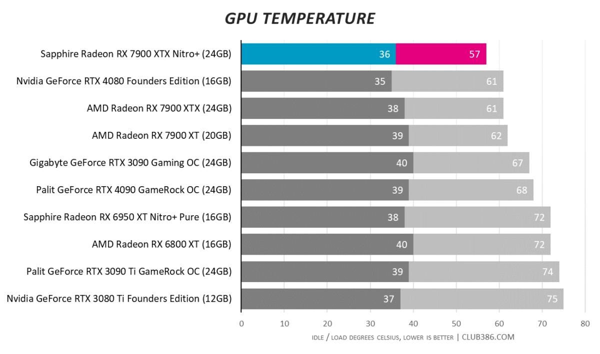
We double-checked figures to ensure the 57°C was accurate. A fantastic return when cooling so many watts, and even the hotspot temperature of 78°C is nothing to worry about.
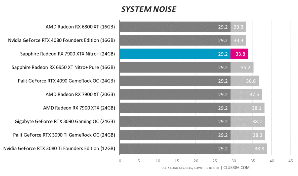
Better still, with the fans running at around 1,600RPM when gaming the card is barely any louder than idle. Extremely cool, extremely quiet. Extremely good.
Overclocking
Here is where it becomes really interesting. Overclocking the latest Radeons is no easy task as there’s no good automated tool. Rather, one needs to increase the maximum power budget by 15 per cent and then, counterintuitively, undervolt the card. This combination allows the GPU to scale frequency as it knows there is power headroom to do so. Increasing clocks farther by pushing sliders to the right leads to a trial-and-error approach.
After a reasonable time fiddling around ensuring frequencies match up to increased performance, we settled on a 3,165MHz boost frequency and memory operating at an effective 22.4Gbps. Here’s how it plays out in select games tested at 4K.
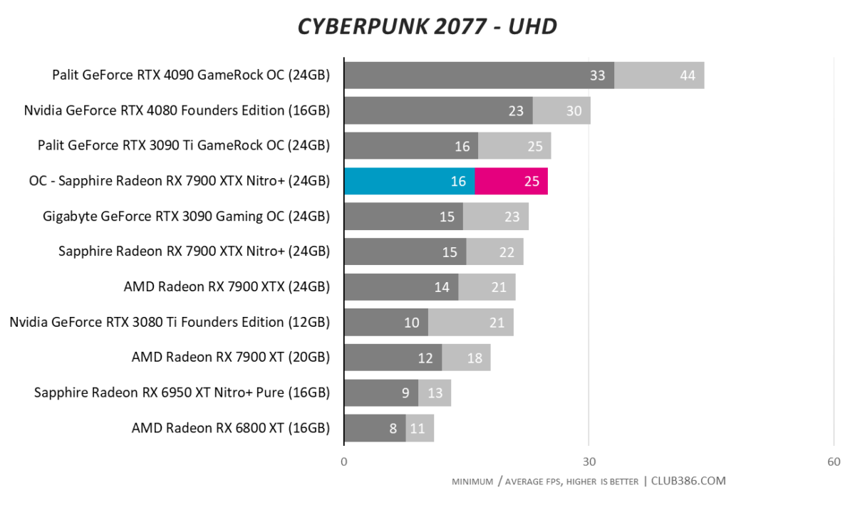
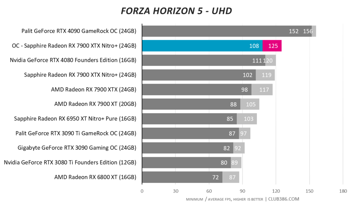
No GeForce RTX 4090-killing performance, but every little helps at 4K.
Conclusion
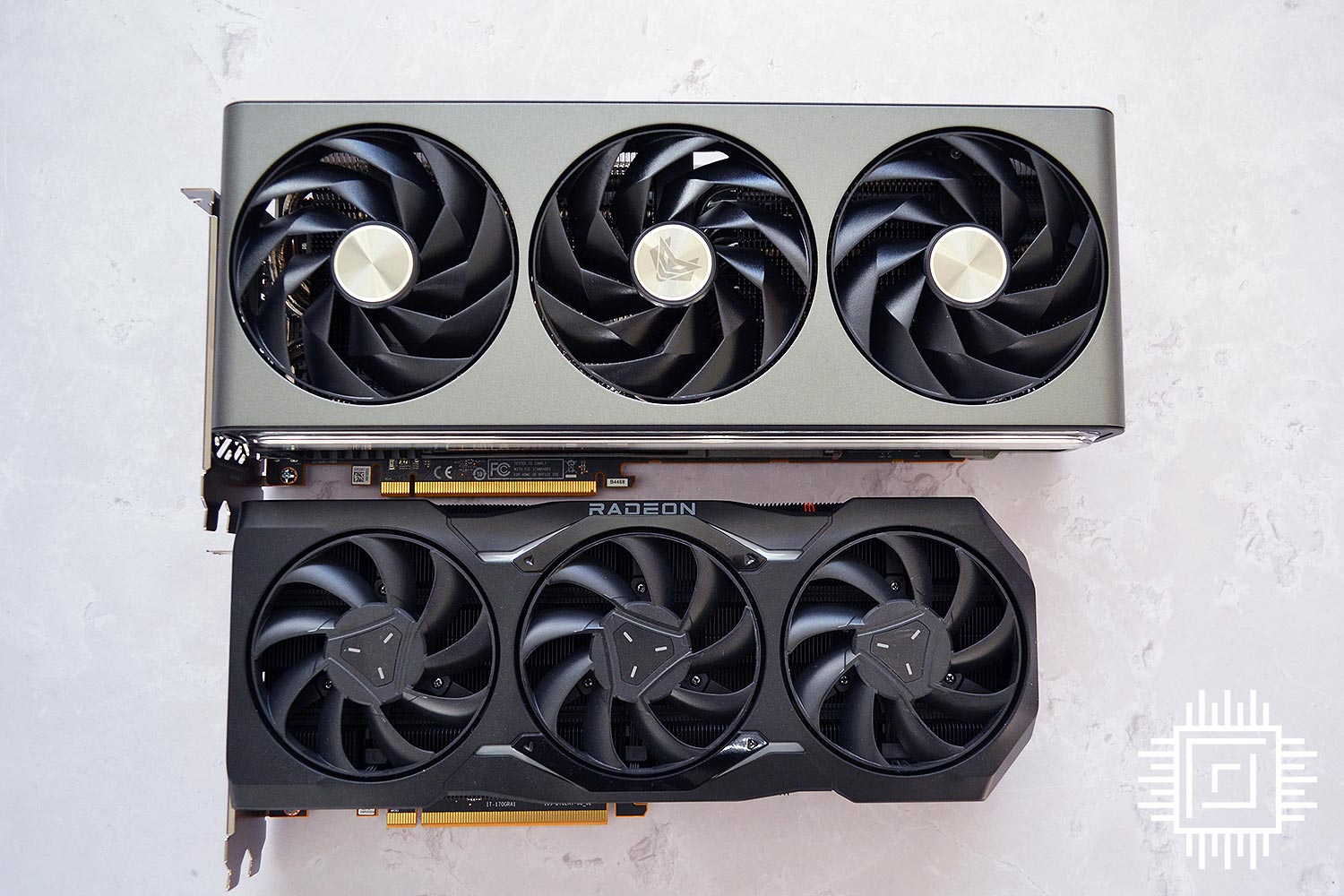
Sapphire understands AMD has raised the bar with in-house Made By AMD reference boards for its latest RDNA 3-powered GPUs. Taking everything good about those cards and adding meaningful upgrades on top leads us to the Nitro+ Vapor-X.
Built like a tank and featuring the most elegant RGB implementation we’ve seen to date, the card is an exercise in less bling meets more style. Underneath that hulking exterior lies top-notch cooling which tames the card’s 420W power budget with ridiculous ease.
Offering up to five per cent extra fps than regular Radeon RX 7900 XTX cards, Sapphire deserves credit for reinventing its design approach in the face of spiralling power budgets and garish competitor cards. The company has left no stone unturned in a quest to build the finest RDNA 3 card possible.
The choice between Radeon RX 7900 XTX and Nvidia GeForce RTX 4080 is a tough one, but if your heart is set going down the AMD route, the big, bold and beautiful Sapphire RX 7900 XTX Nitro+ Vapor-X is the one to get.
Verdict: Refinement and superb performance in a classy package, Sapphire comes up trumps again.

